HDL for synthesis · Lesson 6 of 14
Combinational logic in Verilog and SystemVerilog
Write muxes, decoders, priority encoders, comparators and adders for FPGAs, and learn to avoid latches, combinational loops and internal tri-states.
What you will learn
- Write multiplexers, decoders, priority encoders, comparators and adders in SystemVerilog
- Explain why an if/else chain implies priority and a case statement on one select does not
- Identify code that infers a latch and fix it with default assignments
- Recognise combinational loops and internal tri-states and replace them with legal structures
- Build and verify a 7-segment display decoder
Before you start
- Verilog and SystemVerilog for synthesis (lesson 4)
- FPGA architecture (lesson 2)
After this lesson you can write the standard combinational building blocks, predict what hardware each coding style produces, and spot the three classic combinational bugs: inferred latches, combinational loops and internal tri-states. Every block is tested exhaustively with a self-checking testbench you can download.
What combinational logic is
A combinational circuit’s outputs depend only on its current inputs. It has no memory and no clock. In an FPGA, synthesis maps it onto look-up tables (LUTs), carry chains and multiplexers in the logic blocks, as described in the architecture lesson.
In SystemVerilog you describe combinational logic in two ways:
assignfor expressions that fit on one line.always_combwith=(blocking) assignments when you needif,caseor loops.
The rule that follows from “no memory”: every output must get a value every time the block runs, on every path through the code. Break that rule and synthesis adds memory in the form of a latch. The section on latches below shows how.
Multiplexers
A multiplexer selects one of several inputs. A 2-to-1 mux fits in an assign:
assign y = sel ? b : a;For more inputs, use case:
module mux4 #(
    parameter int WIDTH = 8
) (
    input  logic [1:0]       sel,
    input  logic [WIDTH-1:0] a,
    input  logic [WIDTH-1:0] b,
    input  logic [WIDTH-1:0] c,
    input  logic [WIDTH-1:0] d,
    output logic [WIDTH-1:0] y
);

    always_comb begin
        case (sel)
            2'd0:    y = a;
            2'd1:    y = b;
            2'd2:    y = c;
            default: y = d;
        endcase
    end

endmodulemux4.sv
The default branch covers sel == 3, and it also covers simulation values such as 2'bx1, so y is always assigned. A 4-to-1 mux of one bit has six inputs (four data, two select), which fits in one 6-input LUT on devices that have them. A wider mux is built from several LUTs plus the dedicated multiplexers some families place between LUTs.
An array index is another way to write a mux. y = data[sel]; where data is an array of words selects one word.
Decoders and encoders
A decoder turns an N-bit code into a one-hot output with 2N bits. With an enable:
always_comb begin
    y = '0;              // default: no output active
    if (en)
        y[sel] = 1'b1;
enddecoder3to8.sv
The default assignment at the top is the pattern you will use in every always_comb block. It guarantees an assigned value, and later lines override it.
An encoder goes the other way: one-hot in, binary out. Real inputs are rarely guaranteed one-hot, so the useful version is the priority encoder, which reports the highest-numbered active input and a valid flag. Two ways to write it:
// 4 inputs with casez: '?' marks bits that do not matter
always_comb begin
    valid = 1'b1;
    casez (req)
        4'b1???: idx = 2'd3;
        4'b01??: idx = 2'd2;
        4'b001?: idx = 2'd1;
        4'b0001: idx = 2'd0;
        default: begin
            idx   = 2'd0;
            valid = 1'b0;
        end
    endcase
end
// 8 inputs with a loop: later iterations overwrite earlier ones,
// so the highest set bit wins
always_comb begin
idx = '0;
valid = 1'b0;
for (int i = 0; i < 8; i++) begin
if (req[i]) begin
idx = 3'(i);
valid = 1'b1;
end
end
endprio_enc4.sv
Download prio_enc8.sv
The loop does not run over time. Synthesis unrolls it into eight if statements, a chain of eight 2-to-1 muxes that it then optimises. The loop version scales to any width with a parameter; the casez version is easier to read for small widths. Use casez with ? rather than casex. casex also treats x values on the input as wildcards, which can hide unknown values during simulation.
Comparators
Equality and magnitude comparisons are operators:
assign eq   = (a == b);
assign lt_u = (a < b);                     // unsigned
assign lt_s = ($signed(a) < $signed(b)); // two's complementcompare.sv
The same bits give different answers for < depending on signedness. For a = 8'hFF and b = 8'h01, lt_u is 0 (255 is not less than 1) and lt_s is 1 (-1 is less than 1). Decide which one you mean and say so in the code. Magnitude comparison is a subtraction internally, so synthesis typically maps it onto the carry chain, the same as an adder.
Adders and the carry chain
A ripple-carry adder chains N full adders. Each full adder computes:
sum  = a ^ b ^ cin
cout = (a & b) | (cin & (a ^ b))
The carry ripples from bit 0 to bit N-1, so the delay grows linearly with the width. On an ASIC that makes ripple carry slow for wide adders, and designers use carry-lookahead or prefix structures instead.
FPGAs solve the problem in hardware. Each logic block contains dedicated carry logic, with a fast dedicated connection to the neighbouring block. Examples are the CARRY4 and CARRY8 primitives in AMD 7-series and UltraScale devices, the adders inside each Intel adaptive logic module (ALM), and SB_CARRY in Lattice iCE40 devices. Synthesis recognises +, - and comparisons and maps them onto this chain. The carry signal never leaves the dedicated path, so a ripple-carry adder on the chain is fast.
The practical rule: write a + b and let synthesis do the rest.
module adder #(
    parameter int WIDTH = 8
) (
    input  logic [WIDTH-1:0] a,
    input  logic [WIDTH-1:0] b,
    input  logic             cin,
    output logic [WIDTH-1:0] sum,
    output logic             cout
);

    assign {cout, sum} = a + b + cin;

endmoduleadder.sv
The left-hand side is WIDTH + 1 bits, so the addition is evaluated at that width and the carry lands in cout. A hand-built lookahead adder made from gates usually ends up in general-purpose LUTs and routing, and is slower and larger than the carry-chain version. How path delay limits the clock frequency is the subject of the timing analysis lesson.
if versus case: priority and parallel logic
An if / else if / else chain tests conditions in order. The first true condition wins, so the conditions have a priority. In hardware that is a cascade of 2-to-1 muxes with the first condition nearest the output.
A case statement on a single select value whose items cannot overlap describes one wide mux. No item has priority over another, because only one can match.
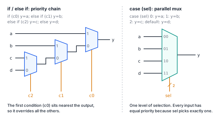
Synthesis tools often simplify a priority chain when they can prove the conditions are mutually exclusive, so the two styles may give the same netlist. The difference matters when the conditions are independent signals, such as several request lines. Then a chain of N conditions adds N levels of logic on the path to the output. Use if when you want priority, and case when you select by one value.
unique case and priority case
SystemVerilog adds keywords that state your assumptions about a case statement:
unique caseasserts that, for every input that occurs, exactly one item matches. The simulator reports a violation if none or more than one matches. Synthesis may use the assumption to build a parallel mux without priority logic.unique0 caseallows no item to match, but still forbids overlaps.priority caseasserts that at least one item matches and that the first match wins. The simulator reports a violation if none matches.
always_comb begin
    y = '0;
    unique case (1'b1)          // one-hot select
        sel_onehot[0]: y = a;
        sel_onehot[1]: y = b;
        sel_onehot[2]: y = c;
    endcase
end
These keywords replace the old // synopsys full_case parallel_case comments. They are safer because a simulator can check the assumption, while the comments only affected synthesis. Simulator support varies: Verilator checks them when you build with --assert, while Icarus Verilog currently ignores them and prints a “sorry” message. They are still a promise. If an input you claimed impossible does occur in hardware, the synthesized logic may do something different from your simulation. Use them only when the promise is true, keep default assignments, and treat every violation message in simulation as a bug.
Unintended latches
This is the most common combinational bug. The following module is wrong on purpose:
// WRONG: infers latches for y and zero
always_comb begin
    case (mode)
        2'd0: begin
            y    = a;
            zero = (a == 8'd0);
        end
        2'd1: y = b;        // zero not assigned
        2'd2: y = a & b;    // zero not assigned
    endcase                 // mode 3: nothing assigned
endlatch_bad.sv (wrong on purpose)
When mode is 1 or 2, the code does not say what zero should be. When mode is 3, it does not say what either output should be. The language semantics are that an unassigned variable keeps its old value. Keeping a value without a clock needs a level-sensitive latch, so synthesis builds one. The synthesis log reports something like “latch inferred for signal zero”; read your synthesis warnings.
Latches cause trouble in FPGAs. Timing analysis through latches is harder to constrain and read. The latch enable here is decoded from mode, so a glitch on mode can open the latch briefly and capture a wrong value. In many families a latch also occupies a storage element that could otherwise hold a flip-flop.
Icarus Verilog compiles this file without a warning. Verilator does not:
%Warning-CASEINCOMPLETE: latch_bad.sv:16:9: Case values incompletely covered (example pattern 0x3)
%Warning-LATCH: latch_bad.sv:15:5: Latch inferred for signal 'y' (not all control paths of combinational always assign a value)
%Warning-LATCH: latch_bad.sv:15:5: Latch inferred for signal 'zero' (not all control paths of combinational always assign a value)
The downloadable latch_bad.sv turns these two warnings off with /* verilator lint_off ... */ comments at the top so it passes the same lint check as the other files. Delete those two lines and lint the file to get the output above.
The fix is a default assignment for every output at the top of the block, plus a default item in the case:
always_comb begin
    y    = '0;      // defaults
    zero = 1'b0;
    case (mode)
        2'd0: begin
            y    = a;
            zero = (a == 8'd0);
        end
        2'd1:    y = b;
        2'd2:    y = a & b;
        default: ;  // mode 3: keep the defaults
    endcase
endlatch_fixed.sv
Defaults at the top work for any amount of nested if and case. You can also write an else and a default everywhere, but in a long block it is easy to miss one. If an output should hold its value between events, that is a register: put it in an always_ff block, as the sequential logic lesson shows.
Combinational loops
A combinational loop is a path from a signal back to itself through logic only, with no register in between. The shortest one is assign x = ~x;, which oscillates. Larger loops are easy to create by accident across two blocks:
// WRONG: y depends on z, and z depends on y
always_comb begin
    if (a) y = b;
    else   y = z;
end
assign z = y & c;
Static timing analysis cannot assign a delay to a path that has no start and end register, and the circuit’s behaviour may depend on routing delays. FPGA tools report combinational loops as warnings or design rule errors. Verilator reports this one as UNOPTFLAT: Circular combinational logic. The fix is to find the feedback path and break it with a register, or to rewrite the logic so the output does not depend on itself.
Tri-states only at I/O pins
Writing 1'bz describes a tri-state driver. Current FPGA families have tri-state buffers only in their I/O blocks. There are no internal tri-state buses, so synthesis either converts an internal tri-state into multiplexers, with a warning, or rejects it. Inside the design, use a mux.
Use tri-state logic only for a top-level bidirectional pin, such as an I2C data line:
module open_drain_pin (
    inout  wire  sda,         // FPGA pin
    input  logic drive_low,   // 1 = pull the line low
    output logic sda_in       // value read back from the pin
);

    assign sda    = drive_low ? 1'b0 : 1'bz;
    assign sda_in = sda;

endmoduleopen_drain_pin.sv
sda is a wire because both the FPGA and external devices drive it. Keep this code at the top level so the z maps directly onto the I/O buffer, and pass plain drive_low and sda_in signals down into the design.
Worked example: a 7-segment decoder
A 7-segment display has segments named a to g. The decoder turns a 4-bit hex value into the segment pattern. Many boards wire the segments active-low (a 0 lights the segment), so this decoder has an active-low output seg_n. Check your board’s schematic.
// Bit order of seg_n: {g, f, e, d, c, b, a}.
//
//      aaa
//     f   b
//      ggg
//     e   c
//      ddd
module seg7_decoder (
    input  logic [3:0] hex,
    output logic [6:0] seg_n
);

    logic [6:0] seg;    // active high: 1 = segment lit

    always_comb begin
        case (hex)          //    gfedcba
            4'h0:    seg = 7'b0111111;
            4'h1:    seg = 7'b0000110;
            4'h2:    seg = 7'b1011011;
            4'h3:    seg = 7'b1001111;
            4'h4:    seg = 7'b1100110;
            4'h5:    seg = 7'b1101101;
            4'h6:    seg = 7'b1111101;
            4'h7:    seg = 7'b0000111;
            4'h8:    seg = 7'b1111111;
            4'h9:    seg = 7'b1101111;
            4'hA:    seg = 7'b1110111;
            4'hB:    seg = 7'b1111100;  // lower-case b
            4'hC:    seg = 7'b0111001;
            4'hD:    seg = 7'b1011110;  // lower-case d
            4'hE:    seg = 7'b1111001;
            default: seg = 7'b1110001;  // F
        endcase
    end

    assign seg_n = ~seg;

endmoduleseg7_decoder.sv
The decoder is written with an internal active-high seg and one inversion at the output. The table then reads naturally (1 = lit), and if your board is active-high you change one line.
A testbench should not copy the RTL table, or it will repeat any typo. This one describes each digit as a string of lit segment letters, such as "abcdg" for 3, builds the expected pattern from the letters, and compares. It also draws each digit in ASCII so you can check the shapes by eye:
2:  _
    _|
   |_
3:  _
    _|
_|tb_seg7.sv
iverilog -g2012 -o sim tb_seg7.sv seg7_decoder.sv && vvp simThe other blocks in this lesson have one exhaustive testbench. It checks every input combination of the mux, decoder, both priority encoders, the 8-bit adder and comparator (all 131072 operand and carry combinations), and the fixed latch example:
Downloadtb_comb.sv
iverilog -g2012 -o sim tb_comb.sv mux4.sv decoder3to8.sv prio_enc8.sv \
    prio_enc4.sv adder.sv compare.sv latch_fixed.sv && vvp sim
For combinational blocks with up to about 20 input bits, exhaustive testing in simulation takes seconds and leaves no case untested.
Remove the latch
This block computes the next value of a counter. Verilator reports LATCH for next. Explain why and fix it so the counter holds its value when neither load nor inc is active.
// WRONG: infers a latch
always_comb begin
    if (load)
        next = din;
    else if (inc)
        next = count + 8'd1;
end
Show solution
When load and inc are both 0, no branch assigns next, so it must keep its old value, which needs a latch. “Hold” for a counter means “next equals the current count”. Assign that as the default:
always_comb begin
    next = count;           // default: hold
    if (load)
        next = din;
    else if (inc)
        next = count + 8'd1;
end
The register itself (count <= next; in an always_ff block) does the holding. The combinational block only computes the value to load.
Add a blanking input to the 7-segment decoder
Write a module seg7_blank with inputs hex[3:0] and blank, and output seg_n[6:0]. When blank is 1 all segments are off; otherwise the output is the normal digit. Reuse seg7_decoder by instantiating it.
Show solution
module seg7_blank (
    input  logic [3:0] hex,
    input  logic       blank,    // 1 = all segments off
    output logic [6:0] seg_n
);

    logic [6:0] digit_n;

    seg7_decoder u_dec (
        .hex   (hex),
        .seg_n (digit_n)
    );

    assign seg_n = blank ? 7'b111_1111 : digit_n;

endmodule
The segments are active-low, so “all off” is all ones. Blanking is useful for suppressing leading zeros on a multi-digit display.
Summary
- Combinational logic has no memory. In
always_comb, give every output a default value at the top so every path assigns it. - Write
a + b,a - band comparisons directly. Synthesis maps them onto the FPGA’s dedicated carry chain, which is faster than hand-built adders. - An
if / else ifchain implies priority; acaseon one select is a parallel mux.uniqueandprioritystate your assumptions and the simulator checks them. - Missing assignments infer latches, and feedback through logic creates combinational loops. Verilator
-Wallreports both asLATCHandUNOPTFLAT. - Use
'zonly on top-level bidirectional pins. Inside the design, use multiplexers. - Small combinational blocks can be tested exhaustively, and the reference model in the testbench should be written independently of the RTL.
Check your understanding
Pick an answer for each question, then check. Answers stay hidden until you submit.
Further reading
- Standard
- Documentation
- Tool
Found a mistake or something unclear?Report a correction.
Follow this course
Get an email when new lessons and projects are added to this course.