Foundations · Lesson 2 of 14
FPGA architecture: LUTs, routing, block RAM and DSP
How an FPGA is built inside: look-up tables, flip-flops, carry chains, routing, block RAM, DSP slices, clock networks, I/O banks and configuration memory.
What you will learn
- Explain how a k-input LUT implements any Boolean function of k inputs and derive the INIT value for a given truth table
- Map vendor names for logic blocks (CLB, slice, ALM, LAB, logic cell) onto the same basic structure
- Explain why carry chains make arithmetic fast and why routing delay depends on placement
- Describe what block RAM, DSP blocks, PLLs and global clock networks provide and when the tools use them
- Explain how I/O banks constrain pin voltages and what configuration memory holds
Before you start
- What is an FPGA (lesson 1)
- Basic digital logic: truth tables, multiplexers, flip-flops
This lesson opens up the blocks you saw in lesson 1. By the end you will be able to work out what a LUT stores for a given function, read vendor block diagrams despite their different naming, and predict which hardware resource the tools will use for a piece of your HDL.
Look-up tables
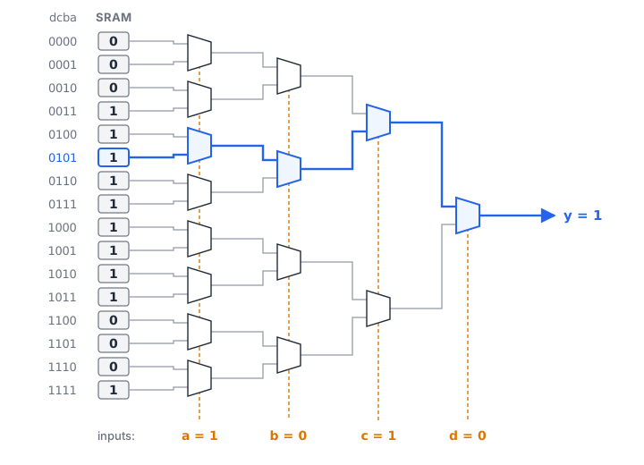
The basic logic element of almost every modern FPGA is the look-up table (LUT). A k-input LUT is a small memory with 2k one-bit cells and a multiplexer tree. The k inputs form an address. The multiplexer tree uses that address to select one stored bit and send it to the output.
Because the stored bits can be anything, a k-input LUT implements every Boolean function of k inputs, with the same delay for a single AND gate as for a complicated expression. What matters is the number of inputs, not the number of gates on paper.
Typical sizes are 4 inputs (Lattice iCE40 and ECP5, Microchip PolarFire, Altera MAX 10) and 6 inputs (AMD 7 series and later). Altera’s adaptive logic module uses a fracturable LUT that can act as one large LUT or as two smaller ones sharing inputs. AMD 6-input LUTs can likewise split into two 5-input LUTs with shared inputs.
Worked example: filling a 4-input LUT
Take the function y = (a & b) | (c ^ d). To configure a LUT for it, evaluate the function for all 16 input combinations. Order the rows by the binary number dcba, so row 0 is all inputs low and row 15 is all inputs high.
| Row | d | c | b | a | a & b | c ^ d | y |
|---|---|---|---|---|---|---|---|
| 0 | 0 | 0 | 0 | 0 | 0 | 0 | 0 |
| 1 | 0 | 0 | 0 | 1 | 0 | 0 | 0 |
| 2 | 0 | 0 | 1 | 0 | 0 | 0 | 0 |
| 3 | 0 | 0 | 1 | 1 | 1 | 0 | 1 |
| 4 | 0 | 1 | 0 | 0 | 0 | 1 | 1 |
| 5 | 0 | 1 | 0 | 1 | 0 | 1 | 1 |
| 6 | 0 | 1 | 1 | 0 | 0 | 1 | 1 |
| 7 | 0 | 1 | 1 | 1 | 1 | 1 | 1 |
| 8 | 1 | 0 | 0 | 0 | 0 | 1 | 1 |
| 9 | 1 | 0 | 0 | 1 | 0 | 1 | 1 |
| 10 | 1 | 0 | 1 | 0 | 0 | 1 | 1 |
| 11 | 1 | 0 | 1 | 1 | 1 | 1 | 1 |
| 12 | 1 | 1 | 0 | 0 | 0 | 0 | 0 |
| 13 | 1 | 1 | 0 | 1 | 0 | 0 | 0 |
| 14 | 1 | 1 | 1 | 0 | 0 | 0 | 0 |
| 15 | 1 | 1 | 1 | 1 | 1 | 0 | 1 |
The LUT contents are the y column. Write it with row 15 as the most significant bit and group it into hexadecimal digits:
rows 15..12: 1 0 0 0  -> 8
rows 11..8:  1 1 1 1  -> F
rows  7..4:  1 1 1 1  -> F
rows  3..0:  1 0 0 0  -> 8
INIT = 16'h8FF8
Vendors call this value INIT (AMD, Lattice) or a LUT mask (Altera). Synthesis computes it, but you will see it in netlists and vendor primitives. The model below works exactly as the hardware does: the four inputs index into the 16-bit INIT parameter. The testbench sets INIT = 16'h8FF8 and checks all 16 rows.
module lut4 #(
  parameter logic [15:0] INIT = 16'h0000
) (
  input  logic a,
  input  logic b,
  input  logic c,
  input  logic d,
  output logic y
);
  assign y = INIT[{d, c, b, a}];
endmodulelut4.sv
Download tb_lut4.sv
Functions with more inputs
A function with more inputs than one LUT is split across several LUTs in levels. Each extra level adds a LUT delay and, more importantly, a trip through the routing. The number of LUT levels between two flip-flops, the logic depth, is therefore a useful first estimate of how fast a path will be.
Flip-flops and the logic block
LUTs are grouped with flip-flops, multiplexers and carry logic into a logic block. The flip-flop sits right after the LUT, so a registered function needs no general routing. A configuration multiplexer selects the LUT result or the registered version, so the same hardware serves combinational and sequential logic.
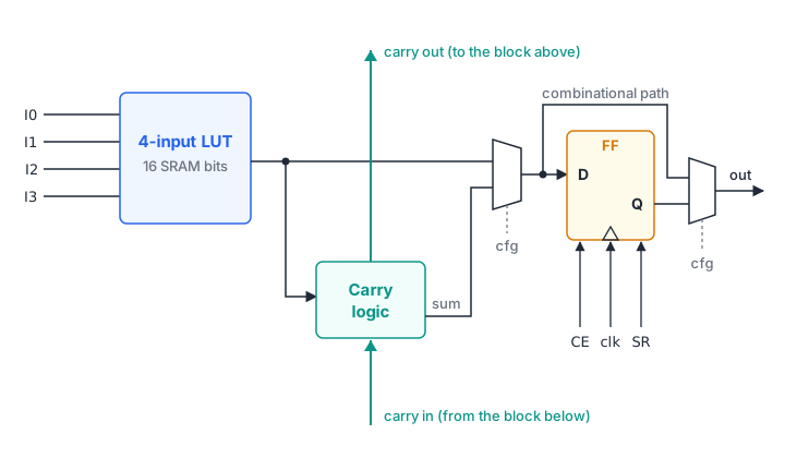
Flip-flops in FPGA fabric usually have a clock enable (CE) and a synchronous or asynchronous set/reset (SR), often shared within a group. In the AMD 7 series, the flip-flops in a slice share one clock and one set/reset signal, so registers with different clocks or resets cannot share a slice. One clock and a consistent reset style help the tools pack logic densely.
Same idea, different names
The table maps each vendor’s names onto the structure in the figure.
| Vendor | Basic cell | Group of cells | Notes |
|---|---|---|---|
| AMD 7 series | 6-input LUT + 2 flip-flops | Slice (4 LUTs, 8 flip-flops); a CLB holds 2 slices | SLICEM slices can also use their LUTs as small RAMs or shift registers |
| Altera Cyclone V and later | Adaptive logic module (ALM): fracturable LUT, adders and registers | Logic array block (LAB) of 10 ALMs | Some LABs (MLABs) can act as small memories |
| Altera MAX 10, Cyclone IV | Logic element (LE): 4-input LUT + 1 register | LAB of 16 LEs | |
| Lattice iCE40 | Logic cell: 4-input LUT + flip-flop + carry | Programmable logic block (PLB) of 8 logic cells | |
| Microchip PolarFire | Logic element: 4-input LUT + flip-flop | Logic cluster | |
| Efinix | XLR cell | Each cell can act as logic or as routing |
Utilisation reports count these cells. Lesson 14 shows how to read them.
Carry chains
Counters, address generators, comparators and accumulators are all adders. A ripple-carry adder computes each sum bit from two input bits and the carry from the bit below, so the carry path through every bit sets the adder’s speed.
If each carry went through general routing, a 32-bit adder would pay 32 routing delays. Instead, FPGAs provide a dedicated carry chain: a hard-wired path from each logic cell to the cell directly above it, with fast carry logic in every cell. The AMD 7 series has carry logic for four bits in each slice, and adjacent slices in a column connect their chains. Altera ALMs contain dedicated adders linked the same way, and every iCE40 logic cell has a carry element.
Synthesis tools map +, - and comparisons onto these chains automatically. The open-source tools show the effect clearly. For a 24-bit counter on a Lattice iCE40UP5K (the blinky design from lesson 3), Yosys 0.66 used 24 LUTs, 24 flip-flops and 22 carry cells, and the critical path report from nextpnr showed each carry hop adding 0.28 ns of logic delay and 0.00 ns of routing delay. Over the whole path, logic accounted for 9.01 ns and routing for 3.54 ns.
That ratio is a property of arithmetic on a carry chain. For general logic the picture reverses.
Routing fabric
The routing fabric connects the blocks. It consists of wire segments of several lengths running in horizontal and vertical channels, connection boxes that link block pins to the channel wires, and switch boxes where channel wires meet and can be joined. Every programmable connection is a switch (a pass transistor or a multiplexer input) controlled by a configuration bit.
Each switch and wire segment adds resistance and capacitance, so every hop adds delay. A signal to a neighbouring block may pass one switch; a signal across the chip passes many. Transistors have improved faster than wires as process nodes shrank, so in modern FPGAs the routing delay on a path is often larger than the logic delay.
- Timing depends on placement. The same netlist can meet timing in one run and fail in another, because the placer put connected blocks further apart.
- High fan-out hurts. A signal that drives hundreds of loads (a reset or an enable, for example) must reach blocks spread across the device and becomes slow. Tools replicate such registers to reduce fan-out.
- Pipelining works. Adding a register in the middle of a long path splits both the logic and the routing delay. Lesson 10 covers how to find the paths that need it.
Routing also takes a large share of the silicon area and of the configuration bits of an FPGA, which is a major reason an FPGA is larger and slower than an ASIC for the same function.
Block RAM
Memories built from flip-flops waste fabric beyond a few dozen bits, so FPGAs include columns of dedicated SRAM blocks:
- Size per block. Examples: 36 Kb in the AMD 7 series (usable as two independent 18 Kb blocks), M10K and M20K blocks in Altera families (10 Kb and 20 Kb), and 4 Kb embedded block RAM in Lattice iCE40. The iCE40 UltraPlus parts add larger single-port SPRAM blocks of 256 Kb each.
- Ports. AMD and Altera block RAMs are true dual-port: two independent ports, each with its own address, data and clock. Others, such as iCE40 block RAM, have one read port and one write port, again with separate clocks. Either way, a block RAM can pass data between two clock domains.
- Aspect ratio. The same block can be deep and narrow or shallow and wide.
- Synchronous read. The read data appears after a clock edge, not combinationally. Your HDL must describe a registered read for the tools to infer block RAM.
- Initial contents. The bitstream can preload the memory, which is how look-up tables and small boot programs are stored.
Many devices can also use LUTs as small memories with combinational read (“distributed RAM” in AMD terms, MLABs in Altera). Lesson 12 shows how to infer each kind.
DSP blocks
Multipliers built from LUTs and carry chains are large and slow. FPGAs include hard DSP blocks that combine a multiplier with adders and registers. The AMD 7 series DSP48E1, for example, contains a 25 × 18-bit signed multiplier, a pre-adder in front of it, and a 48-bit accumulator after it. UltraScale devices widen the multiplier to 27 × 18 bits. Altera’s variable-precision DSP blocks support several multiplier sizes, up to 27 × 27 bits. The iCE40 UltraPlus devices have 16 × 16-bit multiply-accumulate blocks.
Each DSP block has optional pipeline registers at its inputs, after the multiplier and at its output. Without them, the multiplier can limit the clock speed of the whole design. Synthesis absorbs registers written next to the multiply into the DSP block. Dedicated cascade paths between DSP blocks make FIR filters efficient.
Clocking resources
A synchronous design assumes every flip-flop sees the clock edge at almost the same time. General routing would make the difference in arrival times, the clock skew, large and unpredictable, so FPGAs include dedicated clock networks.
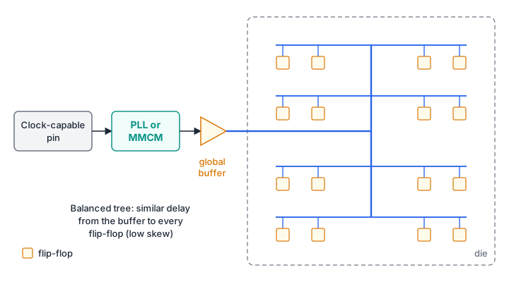
- Clock-capable pins connect directly to the clock network and the PLLs. The board’s oscillator goes to one of them.
- Global clock buffers (BUFG in AMD devices) drive a balanced tree that reaches every region of the chip with low skew. Each device has a limited number of them.
- Regional or local clock networks serve part of the die and are used for I/O interfaces.
- PLLs and MMCMs (mixed-mode clock managers, AMD’s name for its more flexible clock tile) multiply, divide and phase-shift an input clock. From a 100 MHz oscillator you can derive, for example, 200 MHz for a fast datapath and 25 MHz for a video interface. A LOCKED output tells the logic when the output clocks are stable.
Do not use a counter bit as a clock. Such a “ripple clock” travels on general routing, has large skew and is hard to constrain. Use a PLL, or keep one clock and add a clock enable that is high once every N cycles (lesson 7).
I/O banks and standards
The I/O pins are grouped into banks. All pins in a bank share one output supply voltage (VCCO on AMD devices), which determines the I/O standards the bank can use. A bank powered at 3.3 V can run LVCMOS33 but not a standard with 1.8 V outputs. The board designer fixes these supplies, and the schematic tells you what each bank supports.
Common standards include:
- LVCMOS33, LVCMOS25, LVCMOS18: single-ended logic at 3.3 V, 2.5 V or 1.8 V. Most LEDs, buttons and simple peripherals on development boards use LVCMOS33.
- LVDS: low-voltage differential signalling on pin pairs, for fast links to ADCs, displays and cameras.
- SSTL and HSTL: terminated standards used for DDR memory interfaces.
Some families divide banks into types. The AMD 7 series has high-range banks that support up to 3.3 V and high-performance banks limited to 1.8 V but faster. In most families each I/O also contains registers, and many add programmable delays and serialisers for high-speed interfaces. Larger devices add multi-gigabit transceivers, separate hard blocks for serial links such as PCI Express and Ethernet.
Every port needs a pin location and an I/O standard in the constraints (lesson 3).
Configuration memory
Every LUT bit, routing switch, multiplexer setting, I/O standard and block RAM initial value is set by a bit in configuration memory. The bitstream is the image of that memory, so it configures the whole device, not only the part your design uses. For the iCE40UP5K blinky in lesson 3, the bitstream file written by icepack was 104,090 bytes for a design that uses 27 of the device’s 5280 logic cells.
SRAM-based devices load the bitstream at power-up from a JTAG cable (during development), an SPI flash chip on the board, or a host processor. Many devices support bitstream compression to shorten loading. Mid-range and high-end parts add encryption and authentication against copying and tampering, and partial reconfiguration, which reloads one region while the rest keeps running.
LUT contents and LUT counts
- Find the 16-bit INIT value for a 4-input LUT that computes the parity
y = a ^ b ^ c ^ d, using the same row ordering as the worked example (row number =dcba). - How many 4-input LUTs, and in how many levels, does an 8-input AND gate need? How many 6-input LUTs?
- A design has a 16-bit counter and a 16 × 16-bit multiplier. Which dedicated resources do you expect synthesis to use for each?
Show solution
- Parity is 1 when an odd number of inputs are 1. Going from row 15 down to row 0, the outputs are
0110 1001 1001 0110, soINIT = 16'h6996. You can check it by changing the INIT value and the reference expression intb_lut4.sv. - With 4-input LUTs: two LUTs each AND four inputs, and a third LUT ANDs their outputs. That is three LUTs in two levels. With 6-input LUTs: one LUT ANDs six inputs and a second ANDs that result with the remaining two inputs. That is two LUTs in two levels.
- The counter uses 16 flip-flops, a carry chain for the increment, and a few LUTs. The multiplier maps to one DSP block on devices whose multipliers are at least 16 × 16 bits wide (AMD 7 series, Altera, iCE40 UltraPlus). On a device without DSP blocks it would be built from LUTs and carry chains and would be much larger.
Summary
- A k-input LUT stores 2k bits and implements any function of k inputs with the same delay. Synthesis computes the INIT value from your HDL.
- LUTs, flip-flops, carry logic and multiplexers form a logic block. Vendors call it a slice and CLB (AMD), an ALM and LAB (Altera), or a logic cell and PLB (Lattice), but the structure is the same.
- Carry chains make arithmetic fast. For general logic, routing delay often exceeds logic delay, so timing depends on placement, fan-out and pipelining.
- Block RAM and DSP blocks are hard resources for memories and multiply-accumulate. You get them by writing HDL in the style the tools recognise.
- Clocks need clock-capable pins, global buffers and PLLs or MMCMs. Do not build clocks from logic.
- I/O banks share a supply voltage that limits which I/O standards can be used together. Configuration memory sets everything, and the bitstream is its image.
Check your understanding
Pick an answer for each question, then check. Answers stay hidden until you submit.
Further reading
- Paper
- Paper
- Paper
- Documentation
- Documentation
Found a mistake or something unclear?Report a correction.
Follow this course
Get an email when new lessons and projects are added to this course.