Building systems · Lesson 14 of 14
FPGA implementation and hardware debug
Read synthesis, place-and-route and timing reports, fix common implementation problems, and debug on the board with ILA, Signal Tap, LEDs and a checklist.
What you will learn
- Read a utilisation report and spot designs that were optimised away or mapped to the wrong resources
- Identify the synthesis and implementation warnings that indicate real bugs, such as inferred latches and unconstrained I/O
- Interpret WNS, TNS, WHS and THS in a timing summary and find unconstrained paths
- Insert an on-chip logic analyser (Vivado ILA or Quartus Signal Tap) and choose probes and triggers
- Work through a systematic checklist when a design works in simulation but not on the board
Before you start
- The FPGA design flow (lesson 3)
- Timing analysis (lesson 10)
- Clock domain crossing (lesson 11)
This lesson covers the work after the RTL is written and simulated: reading what the tools report, fixing the problems they find, and tracking down bugs that only appear in hardware. You will finish with a bring-up design for a new board and a checklist for designs that work in simulation but not on the board.
Reading the synthesis report
Two parts of the synthesis log deserve attention on every build: the utilisation summary and the warnings.
Utilisation
The utilisation report counts LUTs, flip-flops, block RAMs, DSP blocks, I/O pins and global clock buffers. In Vivado run report_utilization; in Quartus read the Analysis and Synthesis and Fitter resource summaries; nextpnr prints a device utilisation table. Compare the numbers with what you expect from the RTL. Large surprises point to a bug.
- Far too small. Synthesis removes logic that does not affect a top-level output. An unconnected output or an unused module result makes everything upstream disappear.
- Far too large. A memory was built from flip-flops instead of block RAM (often a combinational read or a reset on the array), or a multiplier from LUTs instead of a DSP block.
- Wrong I/O count. Bonded I/O should equal the number of top-level port bits.
Warnings worth acting on
Most synthesis warnings are harmless, but some always indicate a bug. Fix or explicitly waive each warning on a new design so that new ones stand out.
| Warning | What it usually means |
|---|---|
| Inferred latch | A combinational block does not assign an output on every path. Almost always unintended. |
| Multiple drivers / multi-driven net | Two processes or assignments drive the same signal. In hardware this is a conflict. |
| Width mismatch or truncation | An assignment loses upper bits, or a constant is wider than its target. |
| Signal or port has no load / removed | Logic is unused. Fine if expected; a bug if it is your main datapath. |
| Input port unconnected or tied to constant | An instance port was left open. Its value in hardware may differ from simulation. |
| Combinational loop | A signal depends on itself without a register. Causes oscillation or unpredictable timing. |
| Black box or missing module | A submodule was not found, so its logic is missing from the netlist. |
Here is a deliberately wrong combinational multiplexer. The case statement has no branch for sel = 3, so y must hold its old value in that case, and holding a value without a clock is a latch.
// WRONG: infers a latch on y because sel = 2'd3 assigns nothing
module mux_bad (
  input  logic [1:0] sel,
  input  logic [7:0] a, b, c,
  output logic [7:0] y
);
  always_comb begin
    case (sel)
      2'd0: y = a;
      2'd1: y = b;
      2'd2: y = c;
    endcase
  end
endmodule
Verilator’s lint run reports both the cause and the effect:
%Warning-CASEINCOMPLETE: mux_bad.sv:8:5: Case values incompletely covered (example pattern 0x3)
%Warning-LATCH: mux_bad.sv:7:3: Latch inferred for signal 'y' (not all control paths of combinational always assign a value)
Yosys stops with an error, because always_comb promises combinational logic:
ERROR: Latch inferred for signal `\mux_bad.\y' from always_comb process ...Written with Verilog’s always @*, the same block passes Yosys 0.66 with only an informational log line, and vendor tools report latches as warnings, not errors. Use always_comb and read the log. The fix is to assign y on every path, here with a default branch:
module mux_fixed (
  input  logic [1:0] sel,
  input  logic [7:0] a, b, c,
  output logic [7:0] y
);
  always_comb begin
    case (sel)
      2'd0:    y = a;
      2'd1:    y = b;
      2'd2:    y = c;
      default: y = '0;   // every path now assigns y
    endcase
  end
endmodule
Lesson 6 covers latch avoidance in more detail.
Place-and-route results
After implementation, check three things before looking at timing.
- Did everything place and route? Expect zero unplaced cells and zero unrouted nets. Vivado’s
report_route_statusshows routing completion. - Is the I/O placement right? Vivado’s
report_ioand the Quartus Fitter pin-out file list every port with its pin, bank and I/O standard. Compare them with the board schematic; a typo in the constraints file is copied faithfully into the design. - How full is the device? A high percentage of slices, CLBs or LABs makes routing and timing closure harder, even if the LUT count looks moderate.
The timing summary
Lesson 10 covers static timing analysis. For a quick check after each build, read these numbers from the Vivado timing summary (report_timing_summary) or the Quartus Timing Analyzer:
| Value | Meaning | Must be |
|---|---|---|
| WNS (worst negative slack) | Smallest setup slack of any path | Zero or positive |
| TNS (total negative slack) | Sum of negative setup slacks over all failing endpoints | Zero |
| WHS (worst hold slack) | Smallest hold slack of any path | Zero or positive |
| THS (total hold slack) | Sum of negative hold slacks | Zero |
A negative WNS means some paths are too slow for the specified clock: the fix is in the RTL (pipelining, less logic depth) or in the constraint, if it was wrong. A negative WHS is more serious because it does not depend on the clock frequency. It usually points to a clocking problem such as a clock on general routing.
Positive slack on every path only means something if every path was checked. Vivado’s check_timing (also part of the timing summary) lists clocks with no definition, register endpoints with no clock, and inputs and outputs with no delay constraints. Quartus has an equivalent unconstrained paths report. An unconstrained clock is not checked at all, so a design can report “timing met” and still fail.
With several clocks, Vivado’s report_clock_interaction shows which clock pairs have paths between them and whether those paths are timed. Every real crossing needs a synchroniser and a constraint (lesson 11).
Common implementation problems
| Symptom | Likely cause | Fix |
|---|---|---|
| Bitstream generation fails with Vivado DRC errors NSTD-1 and UCIO-1 | Ports without an I/O standard (NSTD-1) or without a pin location (UCIO-1) | Add the missing lines to the XDC. Do not downgrade the DRC to a warning. |
| Placement error about an I/O standard or voltage conflict | Two ports in one bank need different supply voltages | Move one port to a bank with the right VCCO, or change the standard. |
| Placement error or warning about clock routing from an I/O pin | Clock input on a pin that is not clock-capable | Use the board’s clock-capable pin. Overriding the check gives a clock with high skew. |
| Timing fails on a path through a high-fan-out net | A reset or enable drives thousands of loads | Register and replicate the signal, or use synchronous resets only where needed. |
| Memory uses thousands of flip-flops | Block RAM not inferred: combinational read, reset on the array, or unsupported port pattern | Rewrite in the vendor’s RAM template style (lesson 12). |
| Long run times or routing congestion | Device nearly full or very wide multiplexers | Reduce logic, pipeline, or choose a larger device. |
Programming the device
Programming problems are usually physical. Work in this order:
- Cable and device detected. If the JTAG scan finds nothing, check power, the USB cable and drivers (on Linux, udev rules for the cable).
- Right device and right file. Select the correct device in a multi-device JTAG chain, and check the bitstream’s timestamp.
- Configuration finished. Most boards have a DONE LED. If it stays off, the bitstream is for a different part or the load failed.
- Persistent configuration. Program the configuration flash and set the board’s configuration mode (often a jumper) to boot from flash.
On-chip logic analysers
An on-chip logic analyser is extra logic added to your design. It samples selected signals (probes) on every cycle of a clock you choose, compares them with a trigger condition, stores a window of samples around the trigger in block RAM, and sends them over JTAG to a waveform viewer.
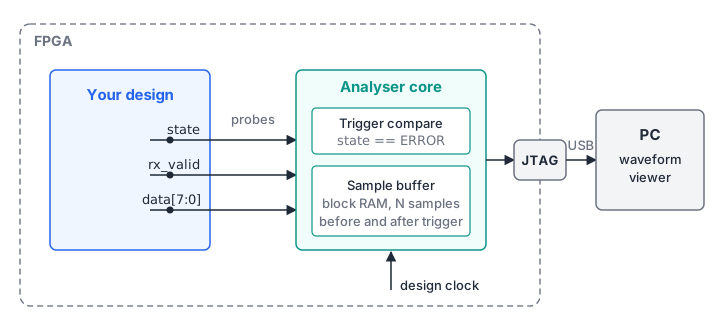
AMD Vivado. Insert the Integrated Logic Analyzer (ILA) by instantiating the ILA IP in your RTL, or mark nets for debug and run the Set Up Debug wizard after synthesis. Mark nets in the HDL with (* mark_debug = "true" *) or in the XDC with set_property MARK_DEBUG true [get_nets btn_sync]. Vivado writes a probes file (.ltx) next to the bitstream, which the Hardware Manager uses to name signals, set triggers and show captures. The Virtual Input/Output (VIO) core lets you read and drive signals from the PC while the design runs.
Altera Quartus. Signal Tap is set up in a Signal Tap file (.stp) added to the project: sample clock, nodes to tap, sample depth and trigger conditions, then a recompile. In-System Sources and Probes plays the role of VIO.
Open-source flows. There is no single standard analyser. Frameworks such as LiteX include one (LiteScope), and a small custom capture buffer read out over a UART works with any toolchain.
Rules for useful captures:
- The sample clock must run. If the clock is missing, the tools cannot detect the debug core. Run the heartbeat test below first.
- Probe registered signals near the problem. Combinational nets can be optimised away; marking a net for debug keeps it.
- Trigger on the error, such as an error state, a FIFO overflow flag or a checksum failure, and keep samples from before it.
- Expect an observer effect. The analyser changes placement and routing. A bug that moves or disappears is almost certainly timing or CDC related.
- Budget block RAM. Sample depth times probe width sets the cost.
LEDs and UART for debug
Before reaching for an analyser, use the outputs every board has. LEDs answer yes/no questions, and a UART (lesson 13) can print counters, state codes and error flags to a terminal.
Worked example: a bring-up design
The first design on a new board should prove that the basics work. This one answers three questions with three LEDs:
- LED0, heartbeat. Blinking at the expected rate proves the bitstream loaded and the clock runs on the right pin at roughly the right frequency.
- LED1, button. Follows a push-button through a two-flop synchroniser, proving the input pin and its constraint.
- LED2, sticky flag. Turns on the first time the button is seen and stays on. Sticky flags catch events too short to see, such as a one-cycle error pulse.
module bringup #(
  parameter int unsigned HB_WIDTH = 27   // 2^26 cycles per toggle at 100 MHz
) (
  input  logic       clk,
  input  logic       btn,   // asynchronous: from a push-button
  output logic [2:0] led
);
  /* verilator lint_off PROCASSINIT */
  logic [HB_WIDTH-1:0] hb_count = '0;
  logic [1:0]          btn_meta = '0;
  logic                seen     = 1'b0;
  /* verilator lint_on PROCASSINIT */

  // mark_debug keeps the net through synthesis so an ILA can probe it.
  (* mark_debug = "true" *) logic btn_sync;

  always_ff @(posedge clk) begin
    hb_count <= hb_count + 1'b1;
  end

  // Two-flop synchroniser for the asynchronous button (lesson 11)
  always_ff @(posedge clk) begin
    btn_meta <= {btn_meta[0], btn};
  end
  assign btn_sync = btn_meta[1];

  // Sticky flag: set once, cleared only by reconfiguring the FPGA
  always_ff @(posedge clk) begin
    if (btn_sync) seen <= 1'b1;
  end

  assign led[0] = hb_count[HB_WIDTH-1];
  assign led[1] = btn_sync;
  assign led[2] = seen;
endmodule
The testbench checks the heartbeat period with a 4-bit counter, the two-edge synchroniser delay, and that led[2] stays set after release. The Basys 3 constraints use pins from Digilent’s master XDC: clock W5, centre button U18, LED0 to LED2 on U16, E19 and U19. The button and LEDs are declared false paths because neither needs I/O timing.
bringup.sv
Download tb_bringup.sv
Download basys3_bringup.xdc
When it works in simulation but not on the board
Check the likely causes in order, cheapest first.
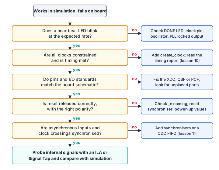
- Clock not running. Check the DONE LED, the clock pin constraint and any PLL’s LOCKED output. Some boards need an oscillator enable pin driven high.
- Timing not met or not checked. Read WNS and WHS, then
check_timing. A design with nocreate_clockhas never been timed. - Wrong pins or I/O standards. Compare the implemented pin report with the schematic. Watch for reversed bit order on vector ports and for active-low buttons or LEDs.
- Reset problems. A reset with the wrong polarity holds the design in reset forever or never resets it. An asynchronous reset released without synchronisation can free some flip-flops a cycle before others. Logic clocked from a PLL should stay in reset until LOCKED is high.
- Clock domain crossing. Simulation rarely shows metastability or skew between bus bits, so unsynchronised crossings pass in simulation and fail at random on the board. Every asynchronous input, including buttons and UART receive lines, needs a synchroniser; multi-bit values need a handshake or an asynchronous FIFO (lesson 11).
- Uninitialised state. Simulation starts an uninitialised register or memory at X; an SRAM-based FPGA starts it at the bitstream value, normally 0; external SDRAM starts with arbitrary contents. A testbench that initialises everything at time zero can hide a missing reset.
- Simulation and synthesis disagree. Delays (
#10),initialblocks that synthesis ignores, incomplete Verilog-2001 sensitivity lists andxcomparisons behave differently in the two. Lint with Verilator and read the synthesis warnings. - Stale bitstream. Change the heartbeat rate or an LED pattern to confirm the new build is loaded.
If all of these pass, insert an ILA or Signal Tap, trigger on the first wrong behaviour, and compare the capture with the same scenario in simulation. The first signal that differs is where to look.
Diagnose a flaky receiver
A UART receiver passes all tests in simulation. On a Basys 3 it receives most characters correctly, but about one character in a few hundred is wrong. The timing summary shows WNS = +2.1 ns and WHS = +0.04 ns. The rx input goes directly from the pin into the receiver’s state machine, which samples it in several states.
- Which item in the checklist is the most likely cause, and why does simulation not show it?
- What change do you make to the RTL?
- You want to confirm the diagnosis with an ILA before changing the design. Which signals do you probe, and what do you trigger on?
Show solution
- Clock domain crossing (item 5). The asynchronous
rxline feeds several state machine flip-flops directly, so occasionally some see the new value and others the old one, or one goes metastable. The simulator changesrxat clean times, and the timing report does not check a path from an unconstrained asynchronous input. - Pass
rxthrough a two-flop synchroniser, asbringup.svdoes for the button, and use only the synchronised signal. Addset_false_path -from [get_ports rx]so the timing report is clean and intentional. - Probe the receiver state, bit counter, received data and data-valid strobe. Trigger on an error, such as a stop bit sampled as 0 (a framing error), and keep most of the window before the trigger. If adding the ILA makes the fault rarer, that is further evidence of a timing or CDC problem.
Summary
- Check utilisation against expectations every build. Far too little logic means outputs are disconnected; far too much means memories or multipliers did not map to hard blocks.
- Treat inferred latches, multiple drivers, truncation, combinational loops and missing modules as bugs. Use
always_combso latches are reported loudly. - WNS, TNS, WHS and THS must all be zero or positive, and
check_timingmust show no unconstrained clocks or endpoints. Unchecked paths are not passing paths. - Bring up a new board with a heartbeat, a synchronised input and a sticky flag before running the real design.
- On-chip logic analysers (Vivado ILA, Quartus Signal Tap) capture internal signals around a trigger; they change placement, so a bug that vanishes when probed points to timing or CDC.
- When simulation passes and hardware fails, check in order: clock, timing constraints, pins, reset, clock domain crossings, initial state, simulation and synthesis mismatches, and the bitstream itself.
Check your understanding
Pick an answer for each question, then check. Answers stay hidden until you submit.
Further reading
- Documentation
- Documentation
- Documentation
- Paper
Found a mistake or something unclear?Report a correction.
Follow this course
Get an email when new lessons and projects are added to this course.