Building systems · Lesson 12 of 14
FPGA memory and DSP: block RAM, FIFOs and MACs
Infer block RAM, distributed RAM and ROM in SystemVerilog, build a synchronous FIFO, and write multiply-accumulate and fixed-point code that maps to DSP slices.
What you will learn
- Choose between registers, distributed RAM, block RAM and large on-chip memories for a given buffer
- Write single-port and simple dual-port RAM and ROM templates that synthesis tools map to block RAM
- Build and verify a synchronous FIFO with correct full, empty and count logic
- Write a pipelined multiply-accumulate that packs into a DSP slice
- Multiply Q1.15 fixed-point numbers with correct rounding and saturation
Before you start
- Sequential logic (lesson 7)
- Testbenches (lesson 9)
- Static timing analysis and timing closure (lesson 10)
After this lesson you can write RAM, ROM and FIFO code that synthesis turns into the FPGA’s dedicated memory blocks, and arithmetic that lands in the DSP slices instead of thousands of LUTs. You will also be able to work in fixed point, which is how most FPGA signal processing represents fractional numbers.
The dedicated blocks were introduced in FPGA architecture. The tools use them only when your code matches what the hardware can do. That is the theme of this lesson: write the hardware’s behaviour, and the tool recognises it.
Where data can live
| Storage | Built from | Read | Typical size per instance | Good for |
|---|---|---|---|---|
| Registers | Flip-flops | Any time, many ports | A few words | Pipeline stages, small register files |
| Distributed RAM | LUTs configured as memory | Asynchronous or synchronous | Tens to a few hundred words | Small buffers, coefficient tables, shallow FIFOs |
| Block RAM | Dedicated RAM blocks | Synchronous only | Hundreds to thousands of words | Line buffers, FIFOs, packet memory |
| Large on-chip RAM | Larger dedicated blocks, in some families | Synchronous only | Much larger than one block RAM | Big frame or lookup buffers |
Distributed RAM uses LUTs as tiny memories. AMD calls the LUTs that can do this SLICEM LUTs; Intel uses MLAB blocks. It is fast and can be read asynchronously, but each bit of storage costs logic.
Block RAM is a hard memory block spread in columns across the die. In AMD 7-series devices each block holds 36 Kb and can be split into two 18 Kb halves. Intel names its blocks by size: M9K in MAX 10, M10K in Cyclone V, M20K in Arria 10, Stratix 10 and Agilex. A block RAM has two ports, a configurable width and depth, an optional output register, and initial contents loaded with the bitstream. Its read is always synchronous: the address is registered on a clock edge and the data appears after it.
Large memories such as AMD UltraRAM (in some UltraScale+ devices) trade flexibility for capacity. They have fewer width options and more restrictions on clocking and initialisation. Check the memory guide for your family before relying on one.
The rule that follows: if you want block RAM, write a synchronous read. An asynchronous read can only be built from LUTs or flip-flops.
Inferring RAM
Synthesis tools recognise a few coding patterns as RAM. Write the memory as an array, write to it in a clocked block, read it in a clocked block, and do not reset the array. A reset on the memory contents rules out block RAM, because the hardware cannot clear all its words in one cycle.
Single-port RAM
One address is used for both reading and writing:
module sp_ram #(
    parameter int DW = 16,   // data width
    parameter int AW = 10    // address width, depth = 2**AW
) (
    input  logic          clk,
    input  logic          en,     // port enable: no read or write when low
    input  logic          we,     // write enable
    input  logic [AW-1:0] addr,
    input  logic [DW-1:0] din,
    output logic [DW-1:0] dout
);
    logic [DW-1:0] mem [0:(1<<AW)-1];

    always_ff @(posedge clk) begin
        if (en) begin
            if (we) begin
                mem[addr] <= din;
            end
            dout <= mem[addr];   // nonblocking: reads the value before this write
        end
    end
endmodulesp_ram.sv
Read-during-write behaviour
When a port writes and reads the same address on the same edge, the output can show three different things. Block RAMs support all three as port modes, and the code you write selects the mode:
- Read-first:
doutshows the old contents. This is the code above. Because both assignments are nonblocking,mem[addr]on the right-hand side is the value before the write. - Write-first (also called read-through):
doutshows the new data. - No-change:
doutkeeps its previous value during writes. This can save power.
Write-first looks like this:
always_ff @(posedge clk) begin
    if (en) begin
        if (we) begin
            mem[addr] <= din;
            dout      <= din;      // new data appears on dout
        end else begin
            dout      <= mem[addr];
        end
    end
end
If the tool cannot match your read-during-write behaviour to a mode the hardware supports, it adds bypass logic around the RAM or uses LUTs instead, and the synthesis log says so. Read the log for every memory you infer.
Simple dual-port RAM
A simple dual-port RAM has one write port and one read port with separate addresses. This is the structure behind most FIFOs and buffers.
always_ff @(posedge clk) begin
    if (we) begin
        mem[waddr] <= din;
    end
end

always_ff @(posedge clk) begin
    if (re) begin
        rd_q <= mem[raddr];
    end
end
The full module adds a parameter OUT_REG. When it is 1, a second register follows the read, so the read latency is two cycles. Block RAMs have this register built in. It shortens the path from the RAM output to the logic that uses the data, because the slow RAM access time is no longer in the same cycle as that logic. When block RAM paths fail timing, turning on the output register is usually the first fix.
sdp_ram.sv
For two clock domains, clock the write block with the write clock and the read block with the read clock. The RAM itself is then the crossing, and the address and control signals still need the treatment in clock domain crossing.
When the write and read addresses are equal on the same edge, the value the read port returns depends on the device and the port mode. If your design can produce that collision and depends on the result, avoid the collision in the control logic or add explicit bypass logic, and check the device memory guide.
ROM from a file
A ROM is a RAM without a write port, with contents loaded at configuration. $readmemh in an initial block reads a hex file at synthesis time. Vivado, Quartus and Yosys all support it.
module rom #(
    parameter int    DW        = 16,
    parameter int    AW        = 6,
    parameter string INIT_FILE = "sine_q15.hex"
) (
    input  logic          clk,
    input  logic [AW-1:0] addr,
    output logic [DW-1:0] dout
);
    logic [DW-1:0] mem [0:(1<<AW)-1];

    initial begin
        $readmemh(INIT_FILE, mem);
    end

    always_ff @(posedge clk) begin
        dout <= mem[addr];
    end
endmodule
The hex file holds one word per line. The example file holds one cycle of a sine wave in 64 samples, in the Q1.15 format explained below. Add the file to the project (or give the path relative to where the tool runs). If synthesis cannot find the file, the ROM contents will be wrong, often with only a warning in the log, so check for it.
Downloadrom.sv
Download sine_q15.hex
Resource hints
You can ask for a specific memory type with an attribute on the array. These are hints: the tool may still refuse if the code does not fit the requested resource.
(* ram_style = "block" *)   logic [15:0] buf_a [0:1023];   // Vivado: "block", "distributed", "registers", "ultra"
(* ramstyle  = "M20K" *)    logic [15:0] buf_b [0:1023];   // Quartus: "M20K" (or M10K, M9K), "MLAB", "logic"
Vivado also has use_dsp for arithmetic, and Quartus has multstyle. Use attributes when the tool’s default choice is wrong, for example a small table that went into block RAM when you need the block RAMs elsewhere.
Synchronous FIFO
A FIFO (first in, first out) buffer passes data between a producer and a consumer that do not run in lock step. The synchronous FIFO here uses one clock for both sides. It is a simple dual-port RAM plus a write pointer, a read pointer and status flags.
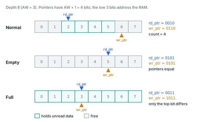
The pointers have one more bit than the RAM address. The low bits address the RAM. The extra top bit flips each time a pointer wraps around, which separates the two cases where the low bits are equal:
- Empty: the pointers are equal, including the top bit. Every word written has been read.
- Full: the low bits are equal and the top bits differ. The write pointer is exactly one lap ahead.
- Count:
wr_ptr - rd_ptr, in modular arithmetic. The extra bit lets it reach the full depth.
assign do_wr = wr_en && !full;
assign do_rd = rd_en && !empty;

// Storage: no reset, so the tool can use RAM primitives.
always_ff @(posedge clk) begin
    if (do_wr) begin
        mem[wr_ptr[AW-1:0]] <= wr_data;
    end
    if (do_rd) begin
        rd_data <= mem[rd_ptr[AW-1:0]];
    end
end

// Pointers.
always_ff @(posedge clk) begin
    if (rst) begin
        wr_ptr <= '0;
        rd_ptr <= '0;
    end else begin
        if (do_wr) wr_ptr <= wr_ptr + 1'b1;
        if (do_rd) rd_ptr <= rd_ptr + 1'b1;
    end
end

assign count = wr_ptr - rd_ptr;
assign empty = (wr_ptr == rd_ptr);
assign full  = (wr_ptr[AW] != rd_ptr[AW]) &&
               (wr_ptr[AW-1:0] == rd_ptr[AW-1:0]);
Points worth checking in any FIFO:
- Writes when full and reads when empty are ignored. The
do_wranddo_rdgates protect the pointers, so a misbehaving producer or consumer cannot corrupt the FIFO. - The read has one cycle of latency.
rd_datais valid on the cycle afterrd_enwas accepted. This keeps the read synchronous, so the storage maps to block RAM. A “first-word fall-through” FIFO shows the next word before it is requested; it needs an extra output register stage and more control logic. - The read and write addresses cannot collide. They are equal only when the FIFO is empty (no read accepted) or full (no write accepted), so there is no read-during-write case to worry about.
- The depth is a power of two, so the pointers wrap naturally.
The testbench keeps a SystemVerilog queue as a reference model. It runs 2000 cycles each of mostly writes, balanced traffic and mostly reads, with random enables. Every cycle it checks full, empty and count against the model, and every read against the expected word. It also checks that the FIFO actually reached full and empty, so a test that never exercised them cannot pass by accident.
sync_fifo.sv
Download tb_sync_fifo.sv
iverilog -g2012 -o sim tb_sync_fifo.sv sync_fifo.sv && vvp sim
# writes 2073, reads 2072, cycles full 1409, cycles empty 1386
# PASS
DSP slices
A DSP slice is a hard arithmetic block: a multiplier, an adder/accumulator behind it, often a pre-adder in front, and pipeline registers at each stage. In AMD 7-series devices the slice (DSP48E1) has a 25 x 18-bit signed multiplier and a 48-bit accumulator. Intel’s variable-precision DSP blocks support several multiplier sizes depending on the family, including a 27 x 27 mode and smaller multipliers around 18 bits wide. A multiply in LUTs costs hundreds of LUTs and is slow; in a DSP slice it costs one block and runs much faster.
The tools put * into DSP slices automatically when the operand widths fit. The challenge is to get the registers into the slice too. The slice’s internal registers sit at fixed points: after the inputs, after the multiplier, and after the adder. If your RTL has registers in the same places, synthesis absorbs them into the slice. If it does not, the multiplier’s full delay ends up in a fabric path, and the design runs far below what the slice can do.
Multiply-accumulate
A multiply-accumulate (MAC) computes every cycle. It is the core of FIR filters, dot products and matrix multiplication.
// Stage 1: input registers.         -> slice input registers
// Stage 2: product register.        -> slice multiplier register
// Stage 3: accumulator register.    -> slice output register
always_ff @(posedge clk) begin
    a_r    <= a;
    b_r    <= b;
    first1 <= first;
    p_r    <= a_r * b_r;
    first2 <= first1;
    if (v2) begin
        acc <= first2 ? ACCW'(p_r) : acc + ACCW'(p_r);
    end
end
The first input starts a new sum: the accumulator loads the product instead of adding it. A separate block, with a reset, moves the valid flags v1, v2 and out_valid along with the data. The latency from inputs to acc is three cycles.
Design choices in this code:
- Data registers have no reset. DSP slice registers typically support only synchronous resets, so an asynchronous reset keeps a register out of the slice. Any reset also adds a load to the reset net. The valid flags tell downstream logic when data is meaningful, so the data does not need a known start value.
- The accumulator has guard bits. A 16 x 16 signed product needs 32 bits. Summing N products needs about more bits. With
ACCW = 40, the 8 guard bits cover at least 256 worst-case products without overflow. - The operands are declared
signed. Mixing signed and unsigned operands makes the whole expression unsigned, as covered in Verilog basics.
The testbench sends 200 dot products of random length (1 to 64 terms) with random idle cycles. It includes the extreme values -32768 and 32767 often, and checks every intermediate accumulator value against a 64-bit reference.
Downloadmac.sv
Download tb_mac.sv
iverilog -g2012 -o sim tb_mac.sv mac.sv && vvp sim
# PASS: 200 sums, 6180 accumulator values checked
After synthesis, check the utilisation report: the MAC should use one DSP slice and almost no LUTs. If it uses LUTs or more slices, look at the operand widths and the register placement first.
Fixed-point arithmetic
FPGAs process fractional numbers mostly in fixed point: an integer with an implied binary point. The notation Qm.n means m integer bits (including the sign bit) and n fractional bits. A Qm.n number is the stored integer divided by .
Q1.15 uses 16 bits: a sign bit and 15 fractional bits. Its range is to , and its resolution is . It is common for audio samples and filter coefficients.
Multiplying Q1.15 numbers
When two fixed-point numbers are multiplied, the integer bits add and the fractional bits add. Q1.15 times Q1.15 gives Q2.30 in 32 bits. To get back to Q1.15 you drop 15 fractional bits, and how you drop them matters.
Worked example: .
- Convert to Q1.15 by multiplying by and rounding:
(
16'h4CCD), and (16'hD333). - Multiply the integers: . In Q2.30 that is . The small difference from comes from rounding the inputs.
- Truncate: an arithmetic shift right by 15 gives (
16'hE51E), which is . Truncation always rounds towards minus infinity. Across many operations, that adds a negative bias. - Round: add half of the result’s LSB, , before the shift. (
16'hE51F), which is . The error against the exact is about , compared with for truncation.
One case overflows: , which Q1.15 cannot represent. The product 16'h8000 * 16'h8000 is , and after the shift it is 32768, one more than the largest Q1.15 value. Saturate it to 16'h7FFF rather than letting it wrap to :
// Q1.15 x Q1.15 -> Q1.15, round half up, saturate
function automatic logic signed [15:0] q15_mul(input logic signed [15:0] a,
                                               input logic signed [15:0] b);
    logic signed [31:0] p;
    p = a * b;                 // Q2.30, exact
    p = p + 32'sd16384;        // add half of the result LSB (2^14)
    p = p >>> 15;              // back to 15 fractional bits
    if (p > 32'sd32767)       return 16'sh7FFF;   // only -1 x -1 gets here
    else if (p < -32'sd32768) return 16'sh8000;
    else                      return p[15:0];
endfunction
Use >>> (arithmetic shift) on a signed value, so the sign bit is copied in from the left. >> would shift in zeros and turn a negative product into a large positive one.
In a filter, do not round after every multiply. Keep the full-precision products in a wide accumulator, as in the MAC above, and round and saturate once at the output. That is both more accurate and cheaper.
Q1.15 by hand
Compute in Q1.15. Give the input integers, the Q2.30 product, and the rounded Q1.15 result in decimal and hex. Then compute and check whether it needs saturation.
Show solution
(16'h6000) and (16'hC000). Both are exact.
Product: , which is in Q2.30.
Rounded: (16'hD000), exactly . No precision is lost because the product’s low 15 bits are zero.
: ; after rounding and the shift, (16'hC000), which is . No saturation is needed. Only overflows.
Add an almost-full flag to the FIFO
Add an output almost_full to sync_fifo that is high when the FIFO holds DEPTH - 2 words or more, where DEPTH = 2**AW. A producer with two cycles of pipeline delay uses it to stop in time. Extend the testbench to check the flag every cycle.
Show solution
The count is already available, so the flag is a comparison:
output logic almost_full,
...
assign almost_full = (count >= (AW+1)'((1 << AW) - 2));
The cast to AW+1 bits matches the width of count and avoids a width warning. For better timing, register the flag: compute it from the next count (current count, plus one if do_wr, minus one if do_rd) and register the comparison, so the output comes straight from a flip-flop.
In the testbench, add a check next to the existing flag checks:
if (almost_full !== (model.size() >= DEPTH - 2)) begin
    $display("ERROR %0t: almost_full=%b, model size %0d", $time, almost_full, model.size());
    errors++;
end
Run it with the three traffic phases. The mostly-write phase drives the count through DEPTH - 2, DEPTH - 1 and DEPTH often, which tests the threshold.
Summary
- Block RAM needs a synchronous read and an array without reset. Asynchronous reads map to distributed RAM or flip-flops.
- The way you write read-during-write selects read-first, write-first or no-change mode. Read the synthesis log to confirm each memory went where you expected.
- A synchronous FIFO is a simple dual-port RAM plus pointers with one extra bit: equal pointers mean empty, a difference only in the top bit means full.
- Put registers before and after the multiplier and after the accumulator so the tool can pack a MAC into one DSP slice. Leave data registers without reset and give the accumulator guard bits.
- Q1.15 times Q1.15 is Q2.30. Round by adding before an arithmetic shift of 15, and saturate the single overflow case, .
- Attributes such as
ram_style,ramstyle,use_dspandmultstyleare hints when the tool’s default resource choice does not suit the design.
Check your understanding
Pick an answer for each question, then check. Answers stay hidden until you submit.
Further reading
- Documentation
Found a mistake or something unclear?Report a correction.
Follow this course
Get an email when new lessons and projects are added to this course.