Foundations · Lesson 3 of 14
The FPGA design flow: from RTL to bitstream
The FPGA design flow step by step: simulation, synthesis, place and route, timing analysis, bitstream and programming, with Vivado, Quartus and Yosys/nextpnr.
What you will learn
- List the steps from specification to a programmed FPGA and the file each step produces
- Explain the feedback loops in the flow and why bugs should be caught in simulation
- Write pin and clock constraints for a simple design in XDC and PCF format
- Build a blinking-LED design with the open-source Yosys and nextpnr flow
- Name the main vendor tools and their constraint file formats
Before you start
- What is an FPGA (lesson 1)
- FPGA architecture (lesson 2)
This lesson walks through every step between an idea and a configured FPGA. By the end you will know what each tool in the chain does, which files it reads and writes, and how to build a blinking LED with both a vendor tool and the open-source flow.
The flow at a glance
The FPGA design flow is a chain of tools, each turning one representation of the design into a more physical one. The figure shows the steps. Three of them check work rather than produce it: simulation, static timing analysis and hardware debug. Each check can send you back to the RTL.
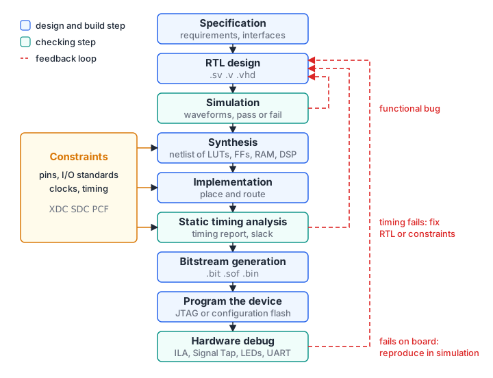
The steps
Specification
Write down what the design must do before writing HDL: interfaces and their protocols, clock frequencies, latency and throughput, the target device and board, and how you will test it. A one-page specification is enough for a small design. It saves time later because the testbench and the constraints both come from it.
RTL design
RTL (register-transfer level) code describes the registers in a design and the combinational logic between them, written in Verilog, SystemVerilog or VHDL. Synthesis tools only accept a subset of each language, the synthesizable subset. Lessons 4 to 8 cover it.
Simulation
A simulator runs your RTL with a testbench that drives inputs and checks outputs. Free simulators include Icarus Verilog, Verilator and GHDL, and every vendor tool includes one (the Vivado simulator, Questa in the Quartus packages). Simulation shows every signal at every time step. Hardware shows you only what reaches a pin. This is why most bugs should be found here. Lesson 9 covers self-checking testbenches.
Functional simulation of RTL does not model gate or wire delays. It tells you whether the logic is correct, not whether it is fast enough.
Synthesis
Synthesis reads the HDL and produces a netlist: a list of device primitives (LUTs, flip-flops, carry cells, block RAMs, DSP blocks, I/O buffers) and the nets that connect them. Along the way it:
- elaborates the design hierarchy and evaluates parameters,
- infers registers, memories, multipliers and state machines from coding patterns,
- optimises the logic and removes anything that does not drive an output,
- maps the result onto the target device’s primitives.
The synthesis report lists the resources used and warnings about things such as inferred latches, multiple drivers and unconnected ports. Lesson 14 explains which warnings to act on.
Implementation: place and route
Implementation turns the netlist into a physical layout. Placement assigns each primitive to a specific site on the die: this LUT to that slice, this RAM to that block RAM column. Routing then chooses which wire segments and switches connect them. Both steps are driven by the timing constraints: the tools try harder to keep critical paths short. Vivado splits implementation into opt_design, place_design, an optional phys_opt_design, and route_design. Quartus calls the whole step the Fitter.
Static timing analysis
Once every wire is known, the timing analyser computes the delay of every path between registers and compares it with the clock period you specified. The difference is the slack. Positive slack means the path is fast enough; negative slack means it is not. Static timing analysis checks every path without needing test vectors, so it complements simulation. Lesson 10 covers it in depth.
Bitstream generation
The bitstream generator turns the placed and routed design into the configuration memory image. Typical output files are .bit from Vivado, .sof from Quartus, and .bin from the iCE40 open-source flow.
Programming the device
There are two ways to load a bitstream into an SRAM-based FPGA:
- JTAG to configuration memory. The PC sends the bitstream over a USB-JTAG cable straight into the FPGA. This is fast and is what you use during development. The configuration is lost at power-off.
- Configuration flash. The bitstream is written to a flash chip on the board, usually SPI flash. At power-up the FPGA reads its configuration from the flash by itself. Vivado writes flash images with
write_cfgmem(.mcsor.bin), and Quartus converts.soffiles into.pofor.jicflash images.
The vendor tools include their own programmers (Vivado Hardware Manager, Quartus Programmer). The open-source openFPGALoader supports many boards from several vendors, and iceprog from Project IceStorm programs iCE40 boards.
Hardware debug
When the design runs on the board you observe it with LEDs, a UART, an oscilloscope, or an on-chip logic analyser such as the Vivado Integrated Logic Analyzer (ILA) or Quartus Signal Tap. Lesson 14 covers these tools and a checklist for the classic “works in simulation, fails on the board” problem.
Iteration loops
The flow is a set of loops, not a straight line. The cost of going around a loop grows with how far down the flow you are. Simulating a small module takes seconds. Synthesis, place and route for a large design can take from minutes to hours. Debugging on hardware is slower still, because you see so little of the design at once.
The practical rule follows: find functional bugs in simulation, find timing problems in the timing report, and use the board to confirm, not to explore. When something fails on the board, reproduce it in simulation before you fix it, so the fix can be verified quickly and the testbench catches the bug if it ever returns.
Constraints and project files
The HDL says what the circuit does. Constraints say how it connects to the outside world and how fast it must run. At minimum, every design needs:
- a pin location for every top-level port,
- an I/O standard for every port (for example LVCMOS33),
- a clock definition with its period for every clock input.
Each tool family has its own file format, though timing constraints in most vendor tools follow the Synopsys Design Constraints (SDC) syntax.
| Tool | Pin and I/O constraints | Timing constraints |
|---|---|---|
| AMD Vivado | XDC (.xdc) | XDC, an SDC-based Tcl format |
| Altera Quartus Prime | Quartus settings file (.qsf) | SDC (.sdc) |
| Lattice Radiant | PDC (.pdc) | SDC (.sdc) |
| Lattice Diamond | LPF (.lpf) | LPF |
| Microchip Libero SoC | PDC (.pdc) | SDC (.sdc) |
| Efinix Efinity | Interface Designer settings | SDC (.sdc) |
| Gowin EDA | CST (.cst) | SDC (.sdc) |
| nextpnr-ice40 | PCF (.pcf) | set_frequency in the PCF, or --freq |
| nextpnr-ecp5 | LPF (.lpf) | LPF FREQUENCY |
Board vendors publish a master constraints file listing every pin on the board. Start from it, uncomment the lines you need, and rename the ports to match your top-level module. That avoids the most common hardware bug: a signal on the wrong pin.
Vendor tools and the open-source flow
Each FPGA vendor supplies its own tool suite, and each offers a free edition or free licence that covers its smaller devices. Check the vendor site for which parts the free edition includes.
| Vendor | Tool | Notes |
|---|---|---|
| AMD | Vivado Design Suite | Vivado ML Standard is the free edition. Tcl-scriptable in project or non-project mode |
| Altera | Quartus Prime | Lite (free), Standard and Pro editions cover different device families |
| Lattice | Radiant, Diamond | Radiant for newer families such as iCE40 UltraPlus and Nexus; Diamond for ECP5 and MachXO |
| Microchip | Libero SoC | For PolarFire, IGLOO 2 and SmartFusion 2 |
| Efinix | Efinity | For Trion and Titanium |
| Gowin | Gowin EDA | For LittleBee and Arora |
The open-source flow covers several Lattice and Gowin families, with growing support for others:
- Yosys synthesises Verilog and much of SystemVerilog for many FPGA families, and produces a JSON netlist.
- nextpnr places and routes that netlist, with timing analysis built in. Separate builds target iCE40 (
nextpnr-ice40), ECP5 (nextpnr-ecp5) and other families. - Bitstream projects document each device family’s configuration format and provide the packers: Project IceStorm for iCE40 (
icepack,iceprog), Project Trellis for ECP5 (ecppack), and Project Apicula for Gowin (gowin_pack). - openFPGALoader programs boards from many vendors over JTAG or SPI.
The open-source tools run quickly and are easy to script, for example in continuous integration. The vendor tools support every device and hard block, and are the only option for most AMD and Altera parts.
Worked example: blinky
The traditional first hardware design blinks an LED. It needs one clock input, one output and one counter. The counter divides the board clock until the LED changes slowly enough to see.
module blinky #(
  parameter int unsigned WIDTH = 27
) (
  input  logic clk,
  output logic led
);
  /* verilator lint_off PROCASSINIT */
  logic [WIDTH-1:0] count = '0;
  /* verilator lint_on PROCASSINIT */

  always_ff @(posedge clk) begin
    count <= count + 1'b1;
  end

  assign led = count[WIDTH-1];
endmodule
The top bit of a WIDTH-bit counter toggles every 2WIDTH-1 clock cycles. With the 100 MHz clock on a Basys 3 and WIDTH = 27, that is every 226 cycles, about 0.67 s. The declaration count = '0 gives the counter a power-up value, which FPGA tools load with the bitstream. The verilator lint_off pragma silences a style warning that Verilator raises because ASIC flows expect a reset instead. Lesson 7 discusses when a design needs a reset.
The testbench uses WIDTH = 4 so the LED toggles every 8 cycles and the check finishes quickly.
blinky.sv
Download tb_blinky.sv
Constraints for the Basys 3 (Vivado)
The Digilent Basys 3 has an AMD Artix-7 XC7A35T in the CPG236 package (Vivado part xc7a35tcpg236-1). According to Digilent’s master XDC file, the 100 MHz oscillator is on pin W5 and LED0 is on pin U16, both in banks powered at 3.3 V.
## 100 MHz clock on pin W5
set_property -dict { PACKAGE_PIN W5   IOSTANDARD LVCMOS33 } [get_ports clk]
create_clock -add -name sys_clk_pin -period 10.00 -waveform {0 5} [get_ports clk]

## LED0 on pin U16
set_property -dict { PACKAGE_PIN U16  IOSTANDARD LVCMOS33 } [get_ports led]

## Configuration bank voltage settings (from the Digilent master file)
set_property CONFIG_VOLTAGE 3.3 [current_design]
set_property CFGBVS VCCO [current_design]
create_clock tells the timing analyser that clk has a 10 ns period. Without it, Vivado has no target to check the design against.
basys3_blinky.xdc
In the Vivado GUI you create a project for part xc7a35tcpg236-1, add the two files, and click Generate Bitstream. The same flow as a non-project Tcl script, run with vivado -mode batch -source build.tcl, shows each step explicitly:
read_verilog -sv blinky.sv
read_xdc basys3_blinky.xdc
synth_design -top blinky -part xc7a35tcpg236-1
opt_design
place_design
route_design
report_utilization    -file utilization.rpt
report_timing_summary -file timing.rpt
write_bitstream -force blinky.bit
Load the result over JTAG with the Vivado Hardware Manager, or with openFPGALoader -b basys3 blinky.bit.
In Quartus the equivalent pin assignments go in the .qsf file as set_location_assignment PIN_xx -to clk and set_instance_assignment -name IO_STANDARD "3.3-V LVTTL" -to clk, where PIN_xx is a placeholder for the pin from your board’s documentation. The clock goes in an .sdc file with create_clock -period 20.000 [get_ports clk] for a 50 MHz oscillator.
The open-source flow on an iCEBreaker
The iCEBreaker board carries a Lattice iCE40UP5K in the SG48 package with a 12 MHz clock on pin 35 and a green LED on pin 37 (from the board’s published PCF file). The PCF for blinky is three lines:
set_io clk 35
set_frequency clk 12
set_io led 37
The LED is active-low, but a blinking LED looks the same either way. At 12 MHz, WIDTH = 24 gives a toggle every 223 cycles, about 0.70 s. The chparam command in Yosys overrides the parameter without editing the source.
# 1. Synthesis: SystemVerilog -> netlist of iCE40 cells (JSON)
yosys -q -l synth.log -p "read_verilog -sv blinky.sv; chparam -set WIDTH 24 blinky; synth_ice40 -top blinky -json blinky.json"

# 2. Place and route, with timing analysis against the 12 MHz target
nextpnr-ice40 --up5k --package sg48 --pcf icebreaker_blinky.pcf \
              --json blinky.json --asc blinky.asc --freq 12

# 3. Bitstream: text configuration (.asc) -> binary (.bin)
icepack blinky.asc blinky.bin

# 4. Program the configuration flash on the board
iceprog blinky.bin
Running steps 1 to 3 with Yosys 0.66 and nextpnr 0.11 produced this summary from nextpnr (excerpt):
Info: Device utilisation:
Info:          ICESTORM_LC:      27/   5280     0%
Info:                SB_IO:       2/     39     5%
Info:                SB_GB:       1/      8    12%
...
Info: Max frequency for clock 'clk$SB_IO_IN_$glb_clk': 79.74 MHz (PASS at 12.00 MHz)
The design uses 27 logic cells, two I/O pins and one global clock buffer. The estimated maximum clock frequency is far above the 12 MHz target, so timing passes. The exact figures will vary slightly between tool versions.
Downloadicebreaker_blinky.pcf
Download build_icebreaker.sh
Two LEDs at two rates
Extend blinky for the Basys 3 so that LED0 blinks as before and LED1 blinks twice as fast.
- Change the module so it has an output
led[1:0], withled[0]as before andled[1]toggling twice as often. - Write the XDC lines for both LEDs. Digilent’s master file puts LED1 on pin E19.
- On a board with a 50 MHz clock, which
WIDTHgives the closest toggle time to 0.5 s forled[0]?
Show solution
- Use the next bit down for the faster LED. No extra counter is needed.
module blinky2 #(
  parameter int unsigned WIDTH = 27
) (
  input  logic       clk,
  output logic [1:0] led
);
  /* verilator lint_off PROCASSINIT */
  logic [WIDTH-1:0] count = '0;
  /* verilator lint_on PROCASSINIT */

  always_ff @(posedge clk) begin
    count <= count + 1'b1;
  end

  assign led[0] = count[WIDTH-1];  // toggles every 2^(WIDTH-1) cycles
  assign led[1] = count[WIDTH-2];  // toggles twice as often
endmodule- With a vector port, each bit needs its own line:
set_property -dict { PACKAGE_PIN U16  IOSTANDARD LVCMOS33 } [get_ports {led[0]}]
set_property -dict { PACKAGE_PIN E19 IOSTANDARD LVCMOS33 } [get_ports {led[1]}]- A 0.5 s toggle at 50 MHz is 25,000,000 cycles. 224 is 16,777,216 cycles (0.34 s) and 225 is 33,554,432 cycles (0.67 s). The closer one is 224, so
WIDTH - 1 = 24andWIDTH = 25.
Summary
- The flow runs specification, RTL, simulation, synthesis, place and route, static timing analysis, bitstream generation, programming and hardware debug.
- Synthesis produces a netlist of device primitives. Implementation places and routes it. Timing analysis checks every path against the clock constraints.
- Each check step can send you back to the RTL, and later loops cost more. Catch functional bugs in simulation.
- Every design needs pin locations, I/O standards and clock definitions. Start from the board’s master constraints file.
- Vendor tools (Vivado, Quartus Prime, Radiant, Diamond, Libero, Efinity, Gowin EDA) support all their devices. The open-source Yosys, nextpnr, IceStorm, Trellis, Apicula and openFPGALoader flow supports several Lattice and Gowin families.
Check your understanding
Pick an answer for each question, then check. Answers stay hidden until you submit.
Further reading
- Paper
- Documentation
- Documentation
- Tool
- Tool
- Tool
Found a mistake or something unclear?Report a correction.
Follow this course
Get an email when new lessons and projects are added to this course.