Building systems · Lesson 13 of 14
FPGA UART project: transmitter, receiver and echo
Build a UART in SystemVerilog: 8N1 framing, baud rate from the system clock, TX and RX state machines, a loopback testbench and a board echo test.
What you will learn
- Calculate the clock divider for a baud rate and the resulting rate error
- Design a UART transmitter and receiver as state machines with mid-bit sampling
- Synchronise an asynchronous serial input and detect framing errors
- Verify TX and RX together with a self-checking loopback testbench
- Constrain the design, program a board and test it from a serial terminal
Before you start
- The FPGA design flow (lesson 3)
- Finite state machines (lesson 8)
- Self-checking testbenches (lesson 9)
- Clock domain crossing (lesson 11)
In this project you build a UART transmitter and receiver, verify them together in a self-checking testbench, and run an echo design on a board: every character you type in a terminal goes to the FPGA and comes straight back. The design uses the state machines from lesson 8, the testbench techniques from lesson 9 and the synchroniser from lesson 11.
What you will build
A UART (universal asynchronous receiver-transmitter) sends bytes one bit at a time over one wire per direction. There is no shared clock: both ends agree on the bit rate in advance and time the bits with their own clocks. A USB-UART bridge, on the board or in an adapter cable, appears on the PC as a serial port, which makes the UART a simple way to talk to an FPGA.
The project has four files:
| File | Contents |
|---|---|
uart_tx.sv | Transmitter: takes a byte with a valid/ready handshake and shifts it out |
uart_rx.sv | Receiver: synchronises the input, finds the start bit, samples each bit in its middle |
uart_echo_top.sv | Top level for a board: RX feeds TX through a one-byte buffer |
tb_uart.sv | Testbench: loopback, framing error, glitch, baud offset and echo tests |
Both TX and RX take two parameters, CLK_FREQ (Hz) and BAUD (bit/s), so the same code works on any board.
The 8N1 frame
“8N1” means 8 data bits, no parity, 1 stop bit, a common default. The line idles high. A frame is:
- One start bit, always 0. Its falling edge tells the receiver that a frame begins.
- Eight data bits, least significant bit first.
- One stop bit, always 1. It returns the line to the idle level, so the next start bit again begins with a falling edge.
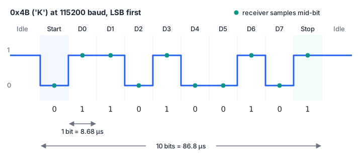
The baud rate is the number of bit periods per second. At 115200 baud, one bit lasts 1 / 115200 s = 8.68 µs and one 10-bit frame lasts 86.8 µs. The highest throughput is 115200 / 10 = 11520 bytes per second, because 2 of every 10 bits are framing.
Baud rate generation
The FPGA times each bit by counting system clock cycles. The number of cycles per bit is the clock frequency divided by the baud rate, rounded to the nearest integer:
In SystemVerilog, with integer parameters, the rounding is done by adding half the divisor before dividing:
localparam int CLKS_PER_BIT = (CLK_FREQ + BAUD / 2) / BAUD;Worked numbers for common clocks:
| Clock | Baud | f_clk / f_baud | N | Actual rate (bit/s) | Error |
|---|---|---|---|---|---|
| 100 MHz | 115200 | 868.06 | 868 | 115207.4 | +0.006 % |
| 50 MHz | 115200 | 434.03 | 434 | 115207.4 | +0.006 % |
| 12 MHz | 115200 | 104.17 | 104 | 115384.6 | +0.16 % |
| 100 MHz | 9600 | 10416.67 | 10417 | 9599.7 | -0.003 % |
| 100 MHz | 921600 | 108.51 | 109 | 917431.2 | -0.45 % |
Rounding is off by at most half a cycle, so the error is small when N is large. Fast baud rates from slow clocks give the largest errors.
How much error is acceptable
The receiver aligns itself to the falling edge of the start bit and then times the rest of the frame with its own clock. Its last sample, in the middle of the stop bit, comes 9.5 of its bit times after that edge. For that sample to land inside the stop bit, 9.5 receiver bit times must lie between 9 and 10 sender bit times. That limits the difference between the two bit rates to about 5 %.
This is a ceiling for the combined error of both ends, not a target. Edge detection latency, slow edges and noise all eat into it, so aim for well below a percent at each end. The testbench in this lesson checks the receiver at ±3 %; in a test run the same receiver also passed at ±4 % and failed at ±5 %.
16x oversampling
Many UART receivers run a tick at 16 times the baud rate, wait 8 ticks from the start edge to reach the middle of the start bit, then sample every 16 ticks. Some take three samples around the middle and use the majority value to reject short noise spikes. The divider is then f_clk / (16 × f_baud), which is much smaller, so the rounding error is larger:
- 100 MHz: 100 000 000 / (16 × 115200) = 54.25, rounded to 54, giving 115741 bit/s, an error of +0.47 %.
- 12 MHz: 12 000 000 / (16 × 115200) = 6.51, rounded to 7, giving 107143 bit/s, an error of -7.0 %. That does not work at all.
The receiver in this lesson counts whole bits at the full clock rate instead, which gives the small errors in the first table. If you need an exact rate from an awkward clock, use a fractional divider: an accumulator that adds a fixed increment every clock and ticks when it overflows. The ticks average to the exact rate, with one clock cycle of jitter.
The transmitter
The transmitter is a four-state FSM: S_IDLE, S_START, S_DATA and S_STOP. A baud counter runs while a frame is in progress and raises bit_done in the last cycle of every bit:
assign bit_done = (baud_cnt == CW'(CLKS_PER_BIT - 1));
assign tx_ready = (state == S_IDLE);

// Baud counter: runs while a frame is being sent, wraps every bit.
always_ff @(posedge clk) begin
    if (rst || state == S_IDLE || bit_done) baud_cnt <= '0;
    else                                    baud_cnt <= baud_cnt + 1'b1;
end
CW is the counter width, $clog2(CLKS_PER_BIT + 1), so the counter is just wide enough for any divider value.
The FSM is written in the one-process style from lesson 8. That makes txd a register, so the serial output cannot glitch. A glitch on txd would look like a start bit to the receiver.
case (state)
    S_IDLE: begin
        txd <= 1'b1;
        if (tx_valid) begin
            shreg <= tx_data;
            txd   <= 1'b0;              // start bit
            state <= S_START;
        end
    end
    S_START: begin
        if (bit_done) begin
            txd     <= shreg[0];        // data bit 0
            shreg   <= {1'b0, shreg[7:1]};
            bit_idx <= 3'd0;
            state   <= S_DATA;
        end
    end
    S_DATA: begin
        if (bit_done) begin
            if (bit_idx == 3'd7) begin
                txd   <= 1'b1;          // stop bit
                state <= S_STOP;
            end else begin
                txd     <= shreg[0];
                shreg   <= {1'b0, shreg[7:1]};
                bit_idx <= bit_idx + 3'd1;
            end
        end
    end
    S_STOP: begin
        if (bit_done) state <= S_IDLE;
    end
    default: state <= S_IDLE;
endcase
The shift register sends the least significant bit first by always outputting shreg[0] and shifting right.
The interface is a valid/ready handshake: the user puts a byte on tx_data and raises tx_valid; the transmitter takes the byte on a clock edge where tx_valid and tx_ready are both high. The user holds tx_valid high until that edge, so no byte is lost, and then drops it or presents the next byte. If the next byte is already waiting when the stop bit ends, the next frame starts one clock later, so frames go out back to back.
uart_tx.sv
The receiver
Input synchroniser
The PC’s UART runs from its own clock, so rxd can change at any moment relative to the FPGA clock. A flip-flop that samples a changing input can go metastable. The receiver passes rxd through two flip-flops and uses only the output of the second, which gives the first a full clock period to settle. Lesson 11 on clock domain crossing explains why this works and how to estimate its reliability.
(* ASYNC_REG = "TRUE" *) logic rx_meta;
(* ASYNC_REG = "TRUE" *) logic rx_sync;

always_ff @(posedge clk) begin
    if (rst) begin
        rx_meta <= 1'b1;                   // line idles high
        rx_sync <= 1'b1;
    end else begin
        rx_meta <= rxd;
        rx_sync <= rx_meta;
    end
end
The ASYNC_REG attribute is for Vivado. It marks the registers as a synchronising chain, so synthesis keeps them and later steps of the flow treat them accordingly. Tools that do not know the attribute ignore it, sometimes with a warning. The registers reset to 1, the idle level, so a reset does not look like a start bit.
The synchroniser delays every edge by the same two clock cycles, so it does not move the sample points relative to the bits.
Finding the middle of each bit
The receiver FSM has the same four states as the transmitter, with a different job in each:
S_IDLE: wait forrx_syncto go low, the start of a start bit.S_START: count half a bit time (CLKS_PER_BIT / 2cycles) to reach the middle of the start bit. If the line is still low, the start bit is real. If it is high again, the low pulse was a glitch and the receiver returns to idle.S_DATA: count one full bit time and sample, eight times. Each sample is taken in the middle of a data bit.S_STOP: count one more bit time and sample the stop bit.
// Wait half a bit, then check that the line is still low.
S_START: begin
    if (baud_cnt == CW'(HALF_BIT - 1)) begin
        baud_cnt <= '0;
        bit_idx  <= 3'd0;
        if (!rx_sync) state <= S_DATA;   // real start bit
        else          state <= S_IDLE;   // glitch: ignore
    end else begin
        baud_cnt <= baud_cnt + 1'b1;
    end
end
// Sample each data bit one full bit time later, mid-bit.
S_DATA: begin
    if (baud_cnt == CW'(CLKS_PER_BIT - 1)) begin
        baud_cnt <= '0;
        shreg    <= {rx_sync, shreg[7:1]};   // LSB first
        if (bit_idx == 3'd7) state <= S_STOP;
        else                 bit_idx <= bit_idx + 3'd1;
    end else begin
        baud_cnt <= baud_cnt + 1'b1;
    end
end
Bits arrive least significant bit first, so each new sample enters at the top of the shift register and moves down. After eight samples, the first bit received is in shreg[0].
Framing errors
// Sample the stop bit mid-bit. Return to idle straight away,
// so the next start bit can be caught early.
S_STOP: begin
    if (baud_cnt == CW'(CLKS_PER_BIT - 1)) begin
        baud_cnt <= '0;
        state    <= S_IDLE;
        if (rx_sync) begin
            rx_data  <= shreg;
            rx_valid <= 1'b1;
        end else begin
            rx_frame_err <= 1'b1;
        end
    end else begin
        baud_cnt <= baud_cnt + 1'b1;
    end
end
A stop bit sampled low is a framing error. The receiver discards the byte and pulses rx_frame_err instead of rx_valid. Common causes are a baud rate mismatch, a receiver that locked onto a data bit instead of a start bit (for example after plugging in the cable mid-transmission), and a break, where the sender holds the line low for longer than a frame. During a break this receiver reports about one framing error per frame time until the line goes high again.
The receiver goes back to S_IDLE in the middle of the stop bit, not at its end. If the sender’s clock is slightly fast, the next start bit can begin before the receiver’s idea of the stop bit has ended. Returning to idle early means the receiver is already waiting for it.
uart_rx.sv
The echo top level
The top level connects RX to TX through a one-byte buffer and adds a reset synchroniser and an error LED.
// Reset synchroniser. FPGA flip-flops load their initial value when the
// device is configured, so the design starts in reset for two cycles.
/* verilator lint_off PROCASSINIT */
logic [1:0] rst_pipe = 2'b11;
/* verilator lint_on PROCASSINIT */
logic       rst;

always_ff @(posedge clk) rst_pipe <= {rst_pipe[0], ~rst_n};
assign rst = rst_pipe[1];
The push button is asynchronous like rxd, so it also goes through two flip-flops. The initial value 2'b11 holds the design in reset right after configuration. Vivado loads such initial values into the flip-flops at configuration, as UG901 describes; with another tool, check that it does the same. Verilator’s lint warns about initial values because ASIC flip-flops have none, and the two comments switch that warning off for this declaration only.
always_ff @(posedge clk) begin
    if (rst) begin
        hold_data <= 8'h00;
        hold_full <= 1'b0;
        led_err   <= 1'b0;
    end else begin
        if (rx_valid) begin
            hold_data <= rx_data;          // a new byte always wins
            hold_full <= 1'b1;
        end else if (hold_full && tx_ready) begin
            hold_full <= 1'b0;             // TX took the byte this cycle
        end
        if (rx_frame_err) led_err <= 1'b1;
    end
end
hold_full drives tx_valid and hold_data drives tx_data. A byte that arrives while TX is busy waits in hold_data. led_err lights after any framing error and stays on until reset, which helps when you hunt for a wrong baud setting.
The one-byte buffer is enough for typing. It has a limit: back-to-back frames from this transmitter are 10 × 868 + 1 = 8681 cycles (86.81 µs), while a PC at exactly 115200 baud starts a frame every 86.806 µs. In a continuous stream of tens of kilobytes the echo falls further behind with every byte and eventually overwrites a byte not yet sent. A FIFO between RX and TX removes that limit; lesson 12 on memory and DSP builds one.
Downloaduart_echo_top.sv
The loopback testbench
The testbench uses the real parameters, 100 MHz and 115200 baud. It connects u_tx to u_rx in loopback, through a multiplexer that also lets the testbench drive the RX input directly. A second pair, the echo top u_top and a monitor receiver u_mon, checks the full echo path. Two checker processes compare every byte from u_rx and u_mon with lists of expected bytes.
The task pc_send generates frames with # delays, as an independent model of a UART transmitter:
task automatic pc_send(input int port, input logic [7:0] b,
                       input int speed, input logic stop_bit);
    set_line(port, 1'b0);                    // start bit
    bit_delay(speed);
    for (int i = 0; i < 8; i++) begin        // data, LSB first
        set_line(port, b[i]);
        bit_delay(speed);
    end
    set_line(port, stop_bit);                // stop bit
    bit_delay(speed);
    set_line(port, 1'b1);                    // idle
endtask
bit_delay waits for the nominal bit time of 8680.56 ns, or 3 % less, or 3 % more. The stop bit value is an argument, so the testbench can also send a bad frame.
The five tests:
- Loopback:
0x00,0xFF,0x55,0xAAand 100 random bytes from a fixed seed, sent back to back throughu_txintou_rx. - Framing error:
pc_sendsends0xA5with a stop bit of 0. Exactly onerx_frame_errpulse and norx_validare expected. - Glitch: a 1 µs low pulse on the idle line, much shorter than half a bit. The receiver must ignore it.
- Baud offset: 10 random bytes sent 3 % fast and 10 sent 3 % slow.
- Echo: the string
"Hello\r\n"sent intou_topmust come back out of it unchanged.
Run it with Icarus Verilog:
iverilog -g2012 -o sim tb_uart.sv uart_tx.sv uart_rx.sv uart_echo_top.sv
vvp sim
Expected output, after a few seconds:
Test 1 loopback:      104 of 104 bytes received
Test 2 framing error: 1 error flagged, no byte output
Test 3 glitch:        ignored
Test 4 baud +/-3 %:   124 of 124 bytes received
Test 5 echo:          7 of 7 bytes echoed
PASS
tb_uart.sv:270: $finish called at 11698641136 (1ps)
The byte counts in test 4 include the 104 bytes from test 1. The simulation covers 11.7 ms of real time. Add +dump to the vvp command to write tb_uart.vcd for a waveform viewer.
All four files pass iverilog -g2012 -Wall and verilator --lint-only -Wall, and the testbench also passes when built with verilator --binary -j 0 --top tb_uart and the same four files.
Check that the tests can fail. Three deliberate bugs, each caught by this testbench: sampling at the start of each bit instead of the middle (set HALF_BIT to 1) fails test 4; sending the most significant bit first fails tests 1 and 5; and ignoring the stop bit fails test 2.
tb_uart.sv
Constraints
Lesson 3 on the design flow explains constraint files. The echo design needs a clock constraint, pin assignments and a decision about timing on the UART pins.
Set CLK_FREQ to your board’s oscillator frequency, in uart_echo_top.sv or as a top-level parameter in your tool. If it is wrong, the baud rate is wrong by the same ratio.
AMD Vivado (XDC). On a Digilent Basys 3, the master XDC file puts the 100 MHz clock on pin W5 and the USB-UART bridge on B18 (RsRx, data into the FPGA) and A18 (RsTx, data out of the FPGA):
set_property -dict { PACKAGE_PIN W5  IOSTANDARD LVCMOS33 } [get_ports clk]
create_clock -add -name sys_clk_pin -period 10.00 -waveform {0 5} [get_ports clk]

set_property -dict { PACKAGE_PIN B18 IOSTANDARD LVCMOS33 } [get_ports uart_rxd]
set_property -dict { PACKAGE_PIN A18 IOSTANDARD LVCMOS33 } [get_ports uart_txd]

# Take the button and LED pins from the master file as well.
# The UART pins have no timing relationship with clk.
set_false_path -from [get_ports {uart_rxd rst_n}]
set_false_path -to   [get_ports {uart_txd led_err}]
Intel Quartus Prime (SDC and pin planner). The clock and false paths use the same SDC commands:
create_clock -name sys_clk -period 20.000 [get_ports clk]
set_false_path -from [get_ports {uart_rxd rst_n}]
set_false_path -to   [get_ports {uart_txd led_err}]
The period here assumes a 50 MHz clock. Assign the pins in the Pin Planner or with set_location_assignment lines in the .qsf file, using the pin names from your board’s manual. Some boards have no USB-UART bridge; on those, connect a 3.3 V USB-UART adapter to header pins.
Open-source flow (iCE40, PCF). On an iCEBreaker, the board’s PCF file puts the 12 MHz clock on pin 35 and the UART on pins 6 (RX, into the FPGA) and 9 (TX, out of the FPGA). Set CLK_FREQ to 12_000_000; from the table above, the divider is 104 and the error is +0.16 %.
set_io clk      35
set_io uart_rxd 6
set_io uart_txd 9
The false paths are correct because the synchroniser handles the asynchronous input and the PC samples uart_txd microseconds after it changes. They also stop the timing report from listing these pins as unconstrained. Lesson 10 on timing analysis covers I/O constraints.
Watch the pin names. A bridge’s TX pin is the FPGA’s receive input. Board files name the pins from one side or the other: in an older Digilent Basys 3 constraints file, pin B18 carries the schematic name UART_TXD_IN (named from the bridge) and the port name RsRx (named from the FPGA). Check which direction each pin is before you assign uart_rxd and uart_txd.
Also check the polarity of the button and LED. rst_n expects a button that reads 0 when pressed, and led_err is high when lit. If your board’s button reads 1 when pressed, or its LED lights on a 0, invert the signal in the top level.
Testing on a board
Wiring and voltage
Boards with a USB-UART bridge on board need only the USB cable that is also used for programming. On the PC, the bridge appears as a serial port: COM3 or similar on Windows (see Device Manager, Ports), /dev/ttyUSB0 or /dev/ttyACM0 on Linux, /dev/cu.usbserial-... or similar on macOS. Some boards’ bridges have two channels, one for programming and one for the UART, and then two ports appear.
With an external adapter, connect adapter TX to uart_rxd, adapter RX to uart_txd, and ground to ground. Use an adapter with 3.3 V logic levels. A PC’s RS-232 port uses higher voltages of both polarities and will damage FPGA pins if connected directly.
Terminal settings
Set the terminal to 115200 baud, 8 data bits, no parity, 1 stop bit, and no flow control.
- screen (Linux, macOS):
screen /dev/ttyUSB0 115200. Quit with Ctrl-A then K. - minicom (Linux):
minicom -D /dev/ttyUSB0 -b 115200. Open the settings with Ctrl-A then O, choose Serial port setup, and turn hardware flow control off. Quit with Ctrl-A then X. - PuTTY (Windows): Connection type Serial, serial line
COM3(your port), speed 115200. Under Connection, Serial, set Flow control to None.
On Linux, opening the port needs permission; on many distributions that means adding your user to the dialout group and logging in again.
What you should see
Terminals do not show what you type unless something sends it back. Every character that appears is therefore one the FPGA received and echoed. Type hello and it appears. Press Enter and the cursor returns to the start of the line, because the terminal sends a carriage return (\r) and the FPGA echoes exactly that.
If something is wrong:
| Symptom | Likely cause |
|---|---|
| Nothing appears | TX and RX swapped, wrong serial port, design held in reset (check button polarity), or the bitstream is not loaded |
| Wrong characters | Baud rate mismatch: wrong CLK_FREQ, or the terminal set to another rate |
led_err lights | Framing errors, usually a baud mismatch |
| Correct characters, but some lost when pasting long text | The one-byte buffer overflowed; add a FIFO |
If the simulation passes and the board does not work, look first at what the simulation does not cover: the constraints, the clock frequency and the pin assignment. Lesson 14 on implementation and debug covers tools for looking inside the running FPGA.
Divider values for other clocks
Calculate CLKS_PER_BIT, the actual bit rate and the error for a 50 MHz clock at 9600 baud and at 921600 baud. Which one would you not use with 16x oversampling, and why?
Show solution
- 9600 baud: 50 000 000 / 9600 = 5208.33, so N = 5208. The actual rate is 50 000 000 / 5208 = 9600.6 bit/s, an error of +0.006 %.
- 921600 baud: 50 000 000 / 921600 = 54.25, so N = 54. The actual rate is 925926 bit/s, an error of +0.47 %.
With 16x oversampling, 921600 baud would need a divider of 54.25 / 16 = 3.39. Rounded to 3, the tick rate is 13 % fast, far outside the 5 % ceiling. At 921600 baud from a 50 MHz clock, count whole bits as this lesson’s receiver does, or use a fractional divider.
Echo in upper case
Change uart_echo_top.sv so that lower-case letters a to z come back as upper case and every other byte is echoed unchanged. Then change the expected bytes in test 5 of the testbench to match and run it.
Show solution
In ASCII, a lower-case letter is the upper-case letter plus 8'h20. Replace the line that loads hold_data:
if (rx_valid) begin
    if (rx_data >= "a" && rx_data <= "z")
        hold_data <= rx_data - 8'h20;   // lower to upper case
    else
        hold_data <= rx_data;
    hold_full <= 1'b1;
end else if (hold_full && tx_ready) begin
In tb_uart.sv, apply the same rule to the expected bytes:
exp_mon[exp_mon_n] = (msg[i] >= "a" && msg[i] <= "z") ? msg[i] - 8'h20 : msg[i];With both changes the testbench prints Test 5 echo: 7 of 7 bytes echoed and PASS, and the modified top level passes verilator --lint-only -Wall. A string literal such as "a" is an 8-bit value in SystemVerilog, so the comparison works directly on the byte.
Summary
- An 8N1 frame is a 0 start bit, 8 data bits LSB first and a 1 stop bit: 10 bits per byte. The line idles high.
- Divide the clock by the baud rate and round to get clocks per bit. At 100 MHz and 115200 baud that is 868, with +0.006 % error. Keep the combined error of both ends far below the 5 % ceiling.
- The transmitter is a four-state FSM with a registered output and a valid/ready handshake. The receiver synchronises
rxdwith two flip-flops, confirms the start bit at its midpoint, samples each bit in the middle and flags a low stop bit as a framing error. - A loopback testbench with an independent frame generator checks normal data, framing errors, glitches, baud offsets and the full echo path at the real clock and baud rate.
- On the board, constrain the clock, assign and check the pins, set the I/O paths as false paths, and test at 115200 8N1 with no flow control.
Check your understanding
Pick an answer for each question, then check. Answers stay hidden until you submit.
Further reading
- Paper
- Documentation
- Documentation
- Documentation
- Tool
Found a mistake or something unclear?Report a correction.
Follow this course
Get an email when new lessons and projects are added to this course.