HDL for synthesis · Lesson 7 of 14
Sequential logic: registers, counters and resets
Build FPGA sequential logic: flip-flops, clock enables, resets, counters, tick generators, shift registers, edge detectors, a debouncer and an LED blinker.
What you will learn
- Write registers with clock enables and synchronous or asynchronous resets
- Explain why FPGA designs use clock enables instead of gated or divided clocks
- Build free-running, modulo-N and prescaler counters with parameterised widths
- Write a shift register, an edge detector and a push-button debouncer
- Build and simulate an LED blinker driven by a tick generator
Before you start
- Verilog and SystemVerilog for synthesis (lesson 4)
- Combinational logic (lesson 6)
After this lesson you can write the sequential building blocks used in almost every FPGA design: registers with enables and resets, counters, tick generators, shift registers, edge detectors and a button debouncer. The lesson ends with an LED blinker you can put on any board. All examples use one clock and update on its rising edge.
Flip-flops and registers
A D flip-flop copies its input d to its output q on the rising clock edge and holds that value until the next edge. A register is a group of flip-flops sharing a clock. In SystemVerilog:
always_ff @(posedge clk)
    q <= d;     // q can be 1 bit or a vector
Every FPGA logic block has flip-flops next to its LUTs, so registers are cheap. In most FPGA families each flip-flop has, in addition to D, Q and the clock, a clock enable input (CE) and a set/reset input. Good sequential code maps directly onto those pins.
For the flip-flop to capture d correctly, d must be stable for a short setup time before the edge and a hold time after it. The timing analysis lesson covers how the tools check this. For now, the rule is simple: all registers in a design use the same clock edge, and everything between registers is combinational logic.
Clock enables, not gated clocks
Often a register should update only on some clock cycles. Use a clock enable:
always_ff @(posedge clk) begin
    if (en)
        q <= d;     // when en is 0, q keeps its value
end
Synthesis connects en to the flip-flop’s CE pin. The register stays on the main clock, and timing analysis treats it like any other register.
The following is wrong in FPGA fabric. It gates the clock with logic:
// WRONG: gated clock built from a LUT
assign gclk = clk & en;
always_ff @(posedge gclk)
    q <= d;
It goes wrong in three ways:
- Glitches. If
enchanges whileclkis high,gclkgets a short extra pulse or a clipped one. The register may capture on an edge that was never meant to exist. - Skew. FPGAs distribute clocks on dedicated low-skew networks.
gclkcomes out of a LUT and travels on general routing, so it arrives later thanclk. Data moving between registers onclkand ongclkcan violate hold time. - Timing analysis. The tools must now treat
gclkas a separate, derived clock. Without extra constraints the analysis is incomplete, and with them the timing is harder to close.
The same problems apply to a clock divided down by a counter (always_ff @(posedge count[7])). If you need a slower rate, generate a one-cycle enable pulse, a tick, as shown below. If a design really must stop a clock, for example to save power, use the vendor’s clock buffer with an enable input (such as BUFGCE on AMD devices) or a clocking block configured by the vendor tools. Never build it from fabric logic.
Synchronous and asynchronous reset
A reset puts registers into a known state. There are two styles.
// Synchronous reset: rst is sampled on the clock edge
always_ff @(posedge clk) begin
    if (rst)
        q_sync <= '0;
    else
        q_sync <= d;
end

// Asynchronous reset: rst_n acts immediately, without a clock edge
always_ff @(posedge clk or negedge rst_n) begin
    if (!rst_n)
        q_async <= '0;
    else
        q_async <= d;
end
A synchronous reset is just another input to the logic in front of the flip-flop. It only works while the clock runs, and timing analysis checks it like any data signal.
An asynchronous reset acts on the flip-flop’s set/reset pin without waiting for a clock edge. Assertion is immediate. Release is the dangerous moment: if the reset input goes inactive close to a clock edge, it violates the flip-flop’s recovery or removal time, which works like setup and hold. Some flip-flops then leave reset one cycle later than others, and some can go metastable. A state machine whose state bits leave reset on different cycles can start in an illegal state.
Vendor guidance differs in the details. AMD’s design guidance favours synchronous resets and recommends resetting only the registers that need it. Intel’s documentation describes a synchronised asynchronous reset: assert asynchronously, release synchronously. Both agree on two points:
- The release of any reset must be synchronised to the clock that the reset registers use.
- Do not reset registers that do not need it. Pipeline and datapath registers that are overwritten with valid data before anyone uses them can stay unreset. Fewer reset connections means less routing, and it lets the tools pack registers into LUT-based shift registers, block RAM and DSP blocks, many of which have restricted or no reset options.
Registers that do need a reset include state machine state, valid flags, counters that set timing, and anything that drives an output pin.
Preview: the reset synchroniser
The standard circuit for rule 1 is a two-flip-flop reset synchroniser. It asserts the reset as soon as the external reset arrives and releases it on a clock edge:
module reset_sync (
    input  logic clk,
    input  logic arst_n,    // asynchronous reset in, active low
    output logic rst_n      // asserts at once, releases on a clock edge
);

    logic [1:0] sync;

    always_ff @(posedge clk or negedge arst_n) begin
        if (!arst_n)
            sync <= 2'b00;
        else
            sync <= {sync[0], 1'b1};
    end

    assign rst_n = sync[1];

endmodule
Each clock domain gets its own copy. The clock domain crossing lesson covers synchronisers in detail.
Initial values in FPGA registers
SRAM-based FPGAs load a value into every flip-flop when the configuration bitstream is loaded. You can choose that value in the HDL:
logic [3:0] count = 4'd0; // value after configurationFPGA synthesis tools generally accept initial values on registers for these devices, which makes them a useful power-up state for simple designs. Three limits apply:
- The value is loaded once, at configuration. It is not a reset. If your design needs to restart without reprogramming the device, it needs a reset.
- ASIC flows and some FPGA families ignore or reject initial values. Check your tool’s documentation before relying on them in code you want to reuse.
- An initial value and a reset value that differ make the design harder to reason about. Keep them the same.
Counters
A counter is a register plus an adder. Synthesis maps the adder onto the carry chain from the combinational logic lesson.
Free-running counter
A free-running counter wraps from all ones to zero by itself, because the addition is modulo 2WIDTH. The counter module from the Verilog lesson is one, with a reset and an enable.
Modulo-N counter
A modulo-N counter counts 0 to N-1 and wraps. It also provides a wrap output, which is the enable for the next counter in a chain (seconds to minutes, for example):
module counter_mod #(
    parameter int N = 10
) (
    input  logic                 clk,
    input  logic                 rst,
    input  logic                 en,
    output logic [$clog2(N)-1:0] count,
    output logic                 wrap
);

    localparam int W = $clog2(N);

    assign wrap = en && (count == W'(N - 1));

    always_ff @(posedge clk) begin
        if (rst)
            count <= '0;
        else if (wrap)
            count <= '0;
        else if (en)
            count <= count + W'(1);
    end

endmodulecounter_mod.sv
$clog2(N) computes the number of bits needed to hold the values 0 to N-1: 4 bits for N = 10, 3 bits for N = 6. It is evaluated at elaboration, so the width follows the parameter.
Prescaler: a tick generator
A prescaler divides the clock rate. Instead of producing a slower clock, it produces a tick: a pulse that is high for exactly one clock cycle every CLK_HZ / TICK_HZ cycles. Other registers use the tick as their clock enable.
module tick_gen #(
    parameter int CLK_HZ  = 100_000_000,
    parameter int TICK_HZ = 1_000
) (
    input  logic clk,
    input  logic rst,     // synchronous, active high
    output logic tick
);

    localparam int DIV = CLK_HZ / TICK_HZ;   // clock cycles per tick
    localparam int W   = (DIV > 1) ? $clog2(DIV) : 1;

    logic [W-1:0] cnt;

    always_ff @(posedge clk) begin
        if (rst) begin
            cnt  <= '0;
            tick <= 1'b0;
        end else if (cnt == W'(DIV - 1)) begin
            cnt  <= '0;
            tick <= 1'b1;
        end else begin
            cnt  <= cnt + W'(1);
            tick <= 1'b0;
        end
    end

endmoduleled_blinker.sv (contains tick_gen)
tick is registered, so it is a clean, glitch-free signal on the main clock. CLK_HZ / TICK_HZ must divide evenly and be at least 2. The waveform shows a counter that increments on each tick when DIV is 4:
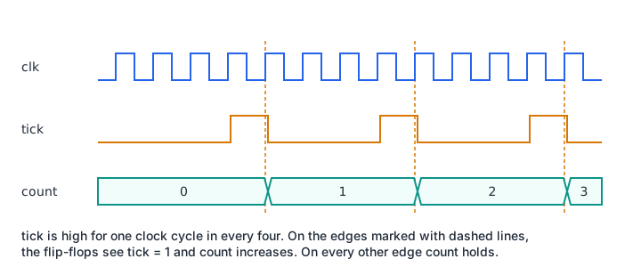
logic [3:0] count;

always_ff @(posedge clk) begin
    if (rst)
        count <= '0;
    else if (tick)
        count <= count + 4'd1;
end
Everything in the design stays on clk. You can chain prescalers: a 1 kHz tick from a 100 MHz clock, then a counter with modulo 1000 enabled by that tick gives a 1 Hz tick.
Shift registers
A shift register moves its contents one position per enabled clock cycle. A serial-in, parallel-out version is the receiving half of a serial link:
module shift_reg #(
    parameter int WIDTH = 8
) (
    input  logic             clk,
    input  logic             en,
    input  logic             din,
    output logic [WIDTH-1:0] q
);

    always_ff @(posedge clk) begin
        if (en)
            q <= {q[WIDTH-2:0], din};
    end

endmoduleshift_reg.sv
The concatenation {q[WIDTH-2:0], din} drops the MSB and inserts din at the LSB. To shift the other way, write {din, q[WIDTH-1:1]}. This module has no reset on purpose. AMD devices, for example, can implement a shift register without reset inside LUTs (SRL primitives) instead of using one flip-flop per bit, which saves registers for long delay lines. A UART, the subject of the UART project, is a typical user of shift registers.
Edge detector
An edge detector produces a one-cycle pulse when a signal changes. Compare the signal with a copy delayed by one register:
module edge_detect (
    input  logic clk,
    input  logic sig,
    output logic rise,
    output logic fall
);

    logic sig_d;    // sig delayed by one clock

    always_ff @(posedge clk)
        sig_d <= sig;

    assign rise =  sig & ~sig_d;
    assign fall = ~sig &  sig_d;

endmoduleedge_detect.sv
rise is high in the one cycle where sig is already 1 but sig_d still holds 0. Use it to start an action once per button press instead of on every cycle the button is held.
sig must already be synchronous to clk. If it comes from a pin, a button or another clock domain, pass it through a synchroniser first. Otherwise sig can change close to the clock edge, sig_d can go metastable, and rise can glitch.
Debouncing a push button
A mechanical button does not switch cleanly. The contacts bounce, so for a few milliseconds after a press or release the input toggles many times. At a 100 MHz clock, that looks like many separate presses. A debouncer accepts a new level only after the input has held it for a set time:
module debounce #(
    parameter int STABLE_CYCLES = 1_000_000
) (
    input  logic clk,
    input  logic rst,       // synchronous, active high
    input  logic btn_raw,   // asynchronous, bouncing input (active high)
    output logic btn        // clean level, synchronous to clk
);

    localparam int W = (STABLE_CYCLES > 1) ? $clog2(STABLE_CYCLES) : 1;

    logic [1:0]   sync;     // two-flip-flop synchroniser
    logic [W-1:0] cnt;

    always_ff @(posedge clk)
        sync <= {sync[0], btn_raw};

    always_ff @(posedge clk) begin
        if (rst) begin
            btn <= 1'b0;
            cnt <= '0;
        end else if (sync[1] == btn) begin
            cnt <= '0;                          // input agrees with output
        end else if (cnt == W'(STABLE_CYCLES - 1)) begin
            btn <= sync[1];                     // stable long enough: accept
            cnt <= '0;
        end else begin
            cnt <= cnt + W'(1);
        end
    end

endmoduledebounce.sv
The design has two stages:
syncis a two-flip-flop synchroniser. The button is asynchronous toclk, and the first flip-flop can go metastable. The second gives it a full clock cycle to settle. The synchroniser has no reset because it does not need one: it fills with valid data after two cycles.- The counter runs only while the synchronised input differs from the output. Any bounce back to the old level clears it. The output changes after
STABLE_CYCLESconsecutive cycles at the new level.
Bounce time depends on the switch. As an example, assume a bounce time below 10 ms: with a 100 MHz clock that is STABLE_CYCLES = 1_000_000. If your board’s button is active-low, invert it at the input: .btn_raw(~btn_n).
Worked example: an LED blinker
The blinker combines a tick generator and a register with an enable. CLK_HZ and BLINK_HZ are parameters, so the same code works on any board and in a fast simulation.
module led_blinker #(
    parameter int CLK_HZ   = 100_000_000,
    parameter int BLINK_HZ = 1
) (
    input  logic clk,
    input  logic rst,     // synchronous, active high
    output logic led
);

    logic tick;

    tick_gen #(
        .CLK_HZ  (CLK_HZ),
        .TICK_HZ (2 * BLINK_HZ)
    ) u_tick (
        .clk  (clk),
        .rst  (rst),
        .tick (tick)
    );

    always_ff @(posedge clk) begin
        if (rst)
            led <= 1'b0;
        else if (tick)
            led <= ~led;
    end

endmoduleled_blinker.sv (led_blinker and tick_gen)
One blink period is one on phase plus one off phase, so the LED toggles at twice the blink rate. With the default parameters, tick_gen counts to 100,000,000 / 2 = 50,000,000. That needs a 26-bit counter, since 225 is about 33.6 million and 226 is about 67.1 million. $clog2 works this out for you.
Simulating 50 million cycles per toggle would be slow. The testbench overrides the parameters instead: CLK_HZ = 1000 and BLINK_HZ = 50 give a toggle every 1000 / 100 = 10 cycles. It measures the spacing of every toggle and fails if any spacing differs:
iverilog -g2012 -o sim tb_led_blinker.sv led_blinker.sv && vvp simPASS: 19 toggles, 10 cycles aparttb_led_blinker.sv
A second testbench checks the modulo counter, the shift register, the edge detector, and the debouncer with a bouncing input:
Downloadtb_seq.sv
To run the blinker on a board, set CLK_HZ to your board’s oscillator frequency, connect rst to a button through a two-flip-flop synchroniser, and map clk and led to pins in the constraints file. Pin constraints are covered in the implementation and debug lesson.
Toggle an LED with a button
Write a module btn_toggle that toggles led once per press of a bouncing push button btn_raw. Reuse debounce and edge_detect. Give it a parameter STABLE_CYCLES that it passes to the debouncer, so you can simulate it with a small value.
Show solution
module btn_toggle #(
    parameter int STABLE_CYCLES = 1_000_000
) (
    input  logic clk,
    input  logic rst,
    input  logic btn_raw,
    output logic led
);

    logic btn, press, release_unused;

    debounce #(.STABLE_CYCLES(STABLE_CYCLES)) u_db (
        .clk     (clk),
        .rst     (rst),
        .btn_raw (btn_raw),
        .btn     (btn)
    );

    edge_detect u_ed (
        .clk  (clk),
        .sig  (btn),
        .rise (press),
        .fall (release_unused)
    );

    always_ff @(posedge clk) begin
        if (rst)
            led <= 1'b0;
        else if (press)
            led <= ~led;
    end

endmodule
The order matters: synchronise, then debounce, then detect the edge. Detecting the edge on the raw input would toggle the LED on every bounce. Simulated with STABLE_CYCLES = 8 and a bouncing input, three presses leave the LED on, as expected.
The edge detector’s fall output is not needed here. Verilator -Wall does not report it as unused because, by default, it ignores signals whose names contain unused.
Replace a divided clock
This code clocks q from bit 7 of a counter, so q increments once every 256 clock cycles. Rewrite it so that every register runs on clk and q increments at the same rate.
// WRONG: q is clocked by a divided clock made in fabric logic
logic [7:0] div;
always_ff @(posedge clk) div <= div + 8'd1;
always_ff @(posedge div[7]) q <= q + 4'd1;
Show solution
Generate a one-cycle tick when the divider reaches its last value and use it as a clock enable. A synchronous reset is added so the simulation starts from a known state:
logic [7:0] div;
logic       tick;

always_ff @(posedge clk) begin
    if (rst)
        div <= '0;
    else
        div <= div + 8'd1;
end

assign tick = (div == 8'hFF);

always_ff @(posedge clk) begin
    if (rst)
        q <= '0;
    else if (tick)
        q <= q + 4'd1;
end
div[7] has one rising edge every 256 cycles, and div == 8'hFF is true for one cycle every 256 cycles, so the rate is the same. Now q sits on the global clock network and timing analysis covers it with no extra constraints.
Summary
- Registers belong in
always_ff @(posedge clk)with non-blocking assignments. Every register in a single-clock design uses the same edge of the same clock. - Slow things down with a clock enable driven by a one-cycle tick, never with a gated or divided clock built from fabric logic.
- Synchronise the release of every reset to its clock, and reset only the registers that need it. Initial values set the state after configuration but do not replace a reset.
- Counters, prescalers and shift registers are a register plus a small piece of logic. Parameterise widths with
$clog2. - External inputs need a synchroniser before any logic uses them. A push button also needs a debouncer, and an edge detector turns a level into a one-cycle event.
- Parameterise clock frequencies so the same RTL runs on a board and in a fast simulation.
Check your understanding
Pick an answer for each question, then check. Answers stay hidden until you submit.
Further reading
- Documentation
- Standard
- Tool
Found a mistake or something unclear?Report a correction.
Follow this course
Get an email when new lessons and projects are added to this course.